HD64F2638F20J Renesas Electronics America, HD64F2638F20J Datasheet - Page 650
HD64F2638F20J
Manufacturer Part Number
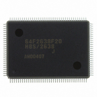
HD64F2638F20J
Description
IC H8S MCU FLASH 256K 128-QFP
Manufacturer
Renesas Electronics America
Series
H8® H8S/2600r
Specifications of HD64F2638F20J
Core Processor
H8S/2600
Core Size
16-Bit
Speed
20MHz
Connectivity
CAN, SCI, SmartCard
Peripherals
Motor Control PWM, POR, PWM, WDT
Number Of I /o
72
Program Memory Size
256KB (256K x 8)
Program Memory Type
FLASH
Ram Size
16K x 8
Voltage - Supply (vcc/vdd)
4.5 V ~ 5.5 V
Data Converters
A/D 12x10b; D/A 2x8b
Oscillator Type
Internal
Operating Temperature
-40°C ~ 85°C
Package / Case
128-QFP
Lead Free Status / RoHS Status
Contains lead / RoHS non-compliant
Eeprom Size
-
Available stocks
Company
Part Number
Manufacturer
Quantity
Price
Company:

Part Number:
HD64F2638F20J
Manufacturer:
PENESAS
Quantity:
252


Section 15 I
(Only for the H8S/2638, H8S/2639, and H8S/2630)
• The I
Table 15-7 Permissible SCL Rise Time (t
IICX
0
1
• The I
Page 600 of 1458
speed mode). In master mode, the I
one bit at a time during communication. If t
the time determined by the input clock of the I
extended. The SCL rise time is determined by the pull-up resistance and load capacitance of
the SCL line. To insure proper operation at the set transfer rate, adjust the pull-up resistance
and load capacitance so that the SCL rise time does not exceed the values given in the table
15-7.
and 300 ns. The I
shown in table 15-6. However, because of the rise and fall times, the I
specifications may not be satisfied at the maximum transfer rate. Table 15-8 shows output
timing calculations for different operating frequencies, including the worst-case influence of
rise and fall times.
t
(a) to provide coding to secure the necessary interval (approximately 1 µs) between issuance of
a stop condition and issuance of a start condition, or (b) to select devices whose input timing
permits this output timing for use as slave devices connected to the I
t
specifications for worst-case calculations of t
investigated include (a) adjusting the rise and fall times by means of a pull-up resistor and
capacitive load, (b) reducing the transfer rate to meet the specifications, or (c) selecting devices
whose input timing permits this output timing for use as slave devices connected to the I
bus.
BUFO
SCLLO
t
Indication
7.5 t
17.5 t
cyc
2
2
fails to meet the I
cyc
C bus interface specification for the SCL rise time t
C bus interface specifications for the SCL and SDA rise and fall times are under 1000 ns
in high-speed mode and t
2
C Bus Interface [Option]
cyc
Standard
mode
High-speed
mode
Standard
mode
High-speed
mode
2
C bus interface SCL and SDA output timing is prescribed by t
2
C bus interface specifications at any frequency. The solution is either
I
Specification
(Max.)
1000 ns
300 ns
1000 ns
300 ns
2
C Bus
STASO
2
C bus interface monitors the SCL line and synchronizes
in standard mode fail to satisfy the I
Sr
φ =
5 MHz
1000 ns
300 ns
1000 ns
300 ns
) Values
sr
Sr
(the time for SCL to go from low to V
Time Indication
2
/t
C bus interface, the high period of SCL is
Sf
. Possible solutions that should be
φ =
8 MHz
937 ns
300 ns
1000 ns
300 ns
sr
is under 1000 ns (300 ns for high-
φ =
10 MHz
750 ns
300 ns
1000 ns
300 ns
2
C bus.
H8S/2639, H8S/2638, H8S/2636,
2
C bus interface
REJ09B0103-0800 Rev. 8.00
H8S/2630, H8S/2635 Group
2
C bus interface
1000 ns 875 ns
φ =
16 MHz
468 ns
300 ns
300 ns
Scyc
IH
and t
May 28, 2010
) exceeds
φ =
20 MHz
375 ns
300 ns
300 ns
2
cyc
C
, as
Related parts for HD64F2638F20J
Image
Part Number
Description
Manufacturer
Datasheet
Request
R


Part Number:
Description:
KIT STARTER FOR M16C/29
Manufacturer:
Renesas Electronics America
Datasheet:

Part Number:
Description:
KIT STARTER FOR R8C/2D
Manufacturer:
Renesas Electronics America
Datasheet:

Part Number:
Description:
R0K33062P STARTER KIT
Manufacturer:
Renesas Electronics America
Datasheet:

Part Number:
Description:
KIT STARTER FOR R8C/23 E8A
Manufacturer:
Renesas Electronics America
Datasheet:

Part Number:
Description:
KIT STARTER FOR R8C/25
Manufacturer:
Renesas Electronics America
Datasheet:

Part Number:
Description:
KIT STARTER H8S2456 SHARPE DSPLY
Manufacturer:
Renesas Electronics America
Datasheet:

Part Number:
Description:
KIT STARTER FOR R8C38C
Manufacturer:
Renesas Electronics America
Datasheet:

Part Number:
Description:
KIT STARTER FOR R8C35C
Manufacturer:
Renesas Electronics America
Datasheet:

Part Number:
Description:
KIT STARTER FOR R8CL3AC+LCD APPS
Manufacturer:
Renesas Electronics America
Datasheet:
Part Number:
Description:
KIT STARTER FOR RX610
Manufacturer:
Renesas Electronics America
Datasheet:

Part Number:
Description:
KIT STARTER FOR R32C/118
Manufacturer:
Renesas Electronics America
Datasheet:

Part Number:
Description:
KIT DEV RSK-R8C/26-29
Manufacturer:
Renesas Electronics America
Datasheet:

Part Number:
Description:
KIT STARTER FOR SH7124
Manufacturer:
Renesas Electronics America
Datasheet:

Part Number:
Description:
KIT STARTER FOR H8SX/1622
Manufacturer:
Renesas Electronics America
Datasheet: