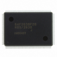
HD64F2638F20J Renesas Electronics America, HD64F2638F20J Datasheet - Page 825

HD64F2638F20J
Manufacturer Part Number
HD64F2638F20J
Description
IC H8S MCU FLASH 256K 128-QFP
Manufacturer
Renesas Electronics America
Series
H8® H8S/2600r
Specifications of HD64F2638F20J
Core Processor
H8S/2600
Core Size
16-Bit
Speed
20MHz
Connectivity
CAN, SCI, SmartCard
Peripherals
Motor Control PWM, POR, PWM, WDT
Number Of I /o
72
Program Memory Size
256KB (256K x 8)
Program Memory Type
FLASH
Ram Size
16K x 8
Voltage - Supply (vcc/vdd)
4.5 V ~ 5.5 V
Data Converters
A/D 12x10b; D/A 2x8b
Oscillator Type
Internal
Operating Temperature
-40°C ~ 85°C
Package / Case
128-QFP
Lead Free Status / RoHS Status
Contains lead / RoHS non-compliant
Eeprom Size
-
Available stocks
Company
Part Number
Manufacturer
Quantity
Price
Company:
Part Number:
HD64F2638F20J
Manufacturer:
PENESAS
Quantity:
252
- Current page: 825 of 1512
- Download datasheet (9Mb)
H8S/2639, H8S/2638, H8S/2636,
H8S/2630, H8S/2635 Group
5. The period for which the P bit in FLMCR1 is set (the write pulse width) should be changed
Item
Wait time after
P bit setting
Note: * Additional programming processing is necessary only when the reprogramming loop count
6. The program/program-verify flowchart for the H8S/2636 is shown in figure 21A-12.
REJ09B0103-0800 Rev. 8.00
May 28, 2010
b. After write pulse application, a verify-read is performed in program-verify mode, and
c. If programming of other bits is incomplete in the 128 bytes, reprogramming processing
according to the degree of progress through the program/program-verify procedure. For
detailed wait time specifications, see section 24.1.7, Flash Memory Characteristics.
To cover the points noted above, bits on which reprogramming processing is to be executed,
and bits on which additional programming is to be executed, must be determined as shown
below.
Since reprogram data and additional-programming data vary according to the progress of the
programming procedure, it is recommended that the following data storage areas (128 bytes
each) be provided in RAM.
programming is judged to have been completed for bits read as 0. The following processing
is necessary for programmed bits.
When programming is completed at an early stage in the program/program-verify
procedure:
If programming is completed in the 1st to 6th reprogramming processing loop, additional
programming should be performed on the relevant bits. Additional programming should
only be performed on bits which first return 0 in a verify-read in certain reprogramming
processing.
When programming is completed at a late stage in the program/program-verify procedure:
If programming is completed in the 7th or later reprogramming processing loop, additional
programming is not necessary for the relevant bits.
should be executed. If a bit for which programming has been judged to be completed is
read as 1 in a subsequent verify-read, a write pulse should again be applied to that bit.
(n) is 1 to 6.
Symbol
t
sp
Item
When reprogramming loop count (n) is 1 to 6
When reprogramming loop count (n) is 7 or more
In case of additional programming processing *
Section 21A ROM
(H8S/2636 Group)
Page 775 of 1458
Symbol
t
t
t
sp30
sp200
sp10
Related parts for HD64F2638F20J
Image
Part Number
Description
Manufacturer
Datasheet
Request
R

Part Number:
Description:
KIT STARTER FOR M16C/29
Manufacturer:
Renesas Electronics America
Datasheet:

Part Number:
Description:
KIT STARTER FOR R8C/2D
Manufacturer:
Renesas Electronics America
Datasheet:

Part Number:
Description:
R0K33062P STARTER KIT
Manufacturer:
Renesas Electronics America
Datasheet:

Part Number:
Description:
KIT STARTER FOR R8C/23 E8A
Manufacturer:
Renesas Electronics America
Datasheet:

Part Number:
Description:
KIT STARTER FOR R8C/25
Manufacturer:
Renesas Electronics America
Datasheet:

Part Number:
Description:
KIT STARTER H8S2456 SHARPE DSPLY
Manufacturer:
Renesas Electronics America
Datasheet:

Part Number:
Description:
KIT STARTER FOR R8C38C
Manufacturer:
Renesas Electronics America
Datasheet:

Part Number:
Description:
KIT STARTER FOR R8C35C
Manufacturer:
Renesas Electronics America
Datasheet:

Part Number:
Description:
KIT STARTER FOR R8CL3AC+LCD APPS
Manufacturer:
Renesas Electronics America
Datasheet:

Part Number:
Description:
KIT STARTER FOR RX610
Manufacturer:
Renesas Electronics America
Datasheet:

Part Number:
Description:
KIT STARTER FOR R32C/118
Manufacturer:
Renesas Electronics America
Datasheet:

Part Number:
Description:
KIT DEV RSK-R8C/26-29
Manufacturer:
Renesas Electronics America
Datasheet:

Part Number:
Description:
KIT STARTER FOR SH7124
Manufacturer:
Renesas Electronics America
Datasheet:

Part Number:
Description:
KIT STARTER FOR H8SX/1622
Manufacturer:
Renesas Electronics America
Datasheet:


