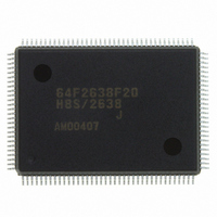
HD64F2638F20J Renesas Electronics America, HD64F2638F20J Datasheet - Page 888

HD64F2638F20J
Manufacturer Part Number
HD64F2638F20J
Description
IC H8S MCU FLASH 256K 128-QFP
Manufacturer
Renesas Electronics America
Series
H8® H8S/2600r
Specifications of HD64F2638F20J
Core Processor
H8S/2600
Core Size
16-Bit
Speed
20MHz
Connectivity
CAN, SCI, SmartCard
Peripherals
Motor Control PWM, POR, PWM, WDT
Number Of I /o
72
Program Memory Size
256KB (256K x 8)
Program Memory Type
FLASH
Ram Size
16K x 8
Voltage - Supply (vcc/vdd)
4.5 V ~ 5.5 V
Data Converters
A/D 12x10b; D/A 2x8b
Oscillator Type
Internal
Operating Temperature
-40°C ~ 85°C
Package / Case
128-QFP
Lead Free Status / RoHS Status
Contains lead / RoHS non-compliant
Eeprom Size
-
Available stocks
Company
Part Number
Manufacturer
Quantity
Price
Company:
Part Number:
HD64F2638F20J
Manufacturer:
PENESAS
Quantity:
252
- Current page: 888 of 1512
- Download datasheet (9Mb)
Section 21B ROM
(H8S/2638 Group, H8S/2639 Group, H8S/2630 Group)
Example in which Flash Memory Block Area EB0 is Overlapped
1. Set bits RAMS, RAM2 to RAM0 in RAMER to 1, 0, 0, 0, to overlap part of RAM onto the
2. Real-time programming is performed using the overlapping RAM.
3. After the program data has been confirmed, the RAMS bit is cleared, releasing RAM overlap.
4. The data written in the overlapping RAM is written into the flash memory space (EB0).
Notes: 1. When the RAMS bit is set to 1, program/erase protection is enabled for all blocks
Page 838 of 1458
H'3FFFF
H'00000
H'01000
H'02000
H'03000
H'04000
H'05000
H'06000
H'07000
H'08000
area (EB0) for which real-time programming is required.
2. A RAM area cannot be erased by execution of software in accordance with the erase
3. Block area EB0 contains the vector table. When performing RAM emulation, the
Flash memory
EB8 to EB11
regardless of the value of RAM2 to RAM0 (emulation protection). In this state, setting
the P or E bit in flash memory control register 1 (FLMCR1), will not cause a transition
to program mode or erase mode. When actually programming or erasing a flash
memory area, the RAMS bit should be cleared to 0.
vector table is needed in the overlap RAM.
algorithm while flash memory emulation in RAM is being used.
EB0
EB1
EB2
EB3
EB4
EB5
EB6
EB7
H8S/2638, H8S/2639
Figure 21B-16 Example of RAM Overlap Operation
This area can be accessed
from both the RAM area
and flash memory area
On-chip RAM
H'FFD000
H'FFDFFF
H'FFEFBF
H'5FFFF
H'00000
H'01000
H'02000
H'03000
H'04000
H'05000
H'06000
H'07000
H'08000
Flash memory
EB8 to EB13
EB0
EB1
EB2
EB3
EB4
EB5
EB6
EB7
H8S/2630
H8S/2639, H8S/2638, H8S/2636,
REJ09B0103-0800 Rev. 8.00
This area can be accessed
from both the RAM area
and flash memory area
H8S/2630, H8S/2635 Group
On-chip RAM
May 28, 2010
H'FFD000
H'FFDFFF
H'FFEFBF
Related parts for HD64F2638F20J
Image
Part Number
Description
Manufacturer
Datasheet
Request
R

Part Number:
Description:
KIT STARTER FOR M16C/29
Manufacturer:
Renesas Electronics America
Datasheet:

Part Number:
Description:
KIT STARTER FOR R8C/2D
Manufacturer:
Renesas Electronics America
Datasheet:

Part Number:
Description:
R0K33062P STARTER KIT
Manufacturer:
Renesas Electronics America
Datasheet:

Part Number:
Description:
KIT STARTER FOR R8C/23 E8A
Manufacturer:
Renesas Electronics America
Datasheet:

Part Number:
Description:
KIT STARTER FOR R8C/25
Manufacturer:
Renesas Electronics America
Datasheet:

Part Number:
Description:
KIT STARTER H8S2456 SHARPE DSPLY
Manufacturer:
Renesas Electronics America
Datasheet:

Part Number:
Description:
KIT STARTER FOR R8C38C
Manufacturer:
Renesas Electronics America
Datasheet:

Part Number:
Description:
KIT STARTER FOR R8C35C
Manufacturer:
Renesas Electronics America
Datasheet:

Part Number:
Description:
KIT STARTER FOR R8CL3AC+LCD APPS
Manufacturer:
Renesas Electronics America
Datasheet:

Part Number:
Description:
KIT STARTER FOR RX610
Manufacturer:
Renesas Electronics America
Datasheet:

Part Number:
Description:
KIT STARTER FOR R32C/118
Manufacturer:
Renesas Electronics America
Datasheet:

Part Number:
Description:
KIT DEV RSK-R8C/26-29
Manufacturer:
Renesas Electronics America
Datasheet:

Part Number:
Description:
KIT STARTER FOR SH7124
Manufacturer:
Renesas Electronics America
Datasheet:

Part Number:
Description:
KIT STARTER FOR H8SX/1622
Manufacturer:
Renesas Electronics America
Datasheet:


