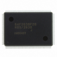
HD64F2638F20J Renesas Electronics America, HD64F2638F20J Datasheet - Page 930

HD64F2638F20J
Manufacturer Part Number
HD64F2638F20J
Description
IC H8S MCU FLASH 256K 128-QFP
Manufacturer
Renesas Electronics America
Series
H8® H8S/2600r
Specifications of HD64F2638F20J
Core Processor
H8S/2600
Core Size
16-Bit
Speed
20MHz
Connectivity
CAN, SCI, SmartCard
Peripherals
Motor Control PWM, POR, PWM, WDT
Number Of I /o
72
Program Memory Size
256KB (256K x 8)
Program Memory Type
FLASH
Ram Size
16K x 8
Voltage - Supply (vcc/vdd)
4.5 V ~ 5.5 V
Data Converters
A/D 12x10b; D/A 2x8b
Oscillator Type
Internal
Operating Temperature
-40°C ~ 85°C
Package / Case
128-QFP
Lead Free Status / RoHS Status
Contains lead / RoHS non-compliant
Eeprom Size
-
Available stocks
Company
Part Number
Manufacturer
Quantity
Price
Company:
Part Number:
HD64F2638F20J
Manufacturer:
PENESAS
Quantity:
252
- Current page: 930 of 1512
- Download datasheet (9Mb)
Section 21C ROM
(H8S/2635 Group)
21C.9.1
When writing data or programs to flash memory, the program/program-verify flowchart shown in
figure 21C-12 should be followed. Performing programming operations according to this
flowchart will enable data or programs to be written to flash memory without subjecting the
device to voltage stress or sacrificing program data reliability. Programming should be carried out
128 bytes at a time.
The wait times after bits are set or cleared in the flash memory control register 1 (FLMCR1) and
the maximum number of programming operations (N) are shown in section 24.2.7, 24.3.7, and
24.4.7, Flash Memory Characteristics.
Following the elapse of (t
is written consecutively to the write addresses. The lower 8 bits of the first address written to must
be H'00 and H'80, 128 consecutive byte data transfers are performed. The program address and
program data are latched in the flash memory. A 128-byte data transfer must be performed even if
writing fewer than 128 bytes; in this case, H'FF data must be written to the extra addresses.
Next, the watchdog timer (WDT) is set to prevent overprogramming due to program runaway, etc.
Set a value greater than (t
entering program mode (program setup) is performed next by setting the PSU bit in FLMCR1. The
operating mode is then switched to program mode by setting the P bit in FLMCR1 after the elapse
of at least (t
Make a program setting so that the time for one programming operation is within the range of
(t
The wait time after P bit setting must be changed according to the degree of progress through the
programming operation. For details see “Notes on Program/Program-Verify Procedure.”
Page 880 of 1458
sp
) µs.
Program Mode
spsu
) µs. The time during which the P bit is set is the flash memory programming time.
sswe
spsu
) µs or more after the SWE bit is set to 1 in FLMCR1, 128-byte data
+ t
sp
+ t
cp
+ t
cpsu
) µs as the WDT overflow period. Preparation for
H8S/2639, H8S/2638, H8S/2636,
REJ09B0103-0800 Rev. 8.00
H8S/2630, H8S/2635 Group
May 28, 2010
Related parts for HD64F2638F20J
Image
Part Number
Description
Manufacturer
Datasheet
Request
R

Part Number:
Description:
KIT STARTER FOR M16C/29
Manufacturer:
Renesas Electronics America
Datasheet:

Part Number:
Description:
KIT STARTER FOR R8C/2D
Manufacturer:
Renesas Electronics America
Datasheet:

Part Number:
Description:
R0K33062P STARTER KIT
Manufacturer:
Renesas Electronics America
Datasheet:

Part Number:
Description:
KIT STARTER FOR R8C/23 E8A
Manufacturer:
Renesas Electronics America
Datasheet:

Part Number:
Description:
KIT STARTER FOR R8C/25
Manufacturer:
Renesas Electronics America
Datasheet:

Part Number:
Description:
KIT STARTER H8S2456 SHARPE DSPLY
Manufacturer:
Renesas Electronics America
Datasheet:

Part Number:
Description:
KIT STARTER FOR R8C38C
Manufacturer:
Renesas Electronics America
Datasheet:

Part Number:
Description:
KIT STARTER FOR R8C35C
Manufacturer:
Renesas Electronics America
Datasheet:

Part Number:
Description:
KIT STARTER FOR R8CL3AC+LCD APPS
Manufacturer:
Renesas Electronics America
Datasheet:

Part Number:
Description:
KIT STARTER FOR RX610
Manufacturer:
Renesas Electronics America
Datasheet:

Part Number:
Description:
KIT STARTER FOR R32C/118
Manufacturer:
Renesas Electronics America
Datasheet:

Part Number:
Description:
KIT DEV RSK-R8C/26-29
Manufacturer:
Renesas Electronics America
Datasheet:

Part Number:
Description:
KIT STARTER FOR SH7124
Manufacturer:
Renesas Electronics America
Datasheet:

Part Number:
Description:
KIT STARTER FOR H8SX/1622
Manufacturer:
Renesas Electronics America
Datasheet:


