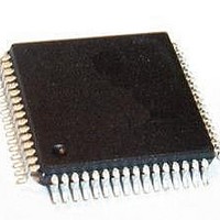
SAK-XC888CLM-8FFA 5V AC Infineon Technologies, SAK-XC888CLM-8FFA 5V AC Datasheet - Page 106

SAK-XC888CLM-8FFA 5V AC
Manufacturer Part Number
SAK-XC888CLM-8FFA 5V AC
Description
IC MCU 8BIT FLASH 64-LQFP
Manufacturer
Infineon Technologies
Series
XC8xxr
Datasheet
1.SAF-XC888CLM-6FFA_5V_AC.pdf
(144 pages)
Specifications of SAK-XC888CLM-8FFA 5V AC
Core Processor
XC800
Core Size
8-Bit
Speed
103.2MHz
Connectivity
CAN, LIN, SSI, UART/USART
Peripherals
Brown-out Detect/Reset, POR, PWM, WDT
Number Of I /o
48
Program Memory Size
32KB (32K x 8)
Program Memory Type
FLASH
Ram Size
1.75K x 8
Voltage - Supply (vcc/vdd)
4.5 V ~ 5.5 V
Data Converters
A/D 8x10b
Oscillator Type
Internal
Operating Temperature
-40°C ~ 125°C
Package / Case
64-LFQFP
Data Bus Width
8 bit
Data Ram Size
1.75 KB
Interface Type
UART, SSC
Maximum Clock Frequency
24 MHz
Number Of Programmable I/os
48
Number Of Timers
4
Operating Supply Voltage
5 V
Maximum Operating Temperature
+ 125 C
Mounting Style
SMD/SMT
Minimum Operating Temperature
- 40 C
On-chip Adc
10 bit, 8 Channel
For Use With
B158-H8743-X-X-7600IN - KIT STARTER XC886/888
Lead Free Status / RoHS Status
Lead free / RoHS Compliant
Eeprom Size
-
Lead Free Status / Rohs Status
Details
Other names
SP000210982
3.21
The XC886/888 includes a high-performance 10-bit Analog-to-Digital Converter (ADC)
with eight multiplexed analog input channels. The ADC uses a successive approximation
technique to convert the analog voltage levels from up to eight different sources. The
analog input channels of the ADC are available at Port 2.
Features
•
•
•
•
•
•
•
•
•
•
•
•
•
•
•
•
•
•
3.21.1
A common module clock
digital parts of the ADC module:
•
•
•
The internal clock for the analog part
Therefore, the ADC clock prescaler must be programmed to a value that ensures
does not exceed 10 MHz. The prescaler ratio is selected by bit field CTC in register
Data Sheet
Successive approximation
8-bit or 10-bit resolution
(TUE of ± 1 LSB and ± 2 LSB, respectively)
Eight analog channels
Four independent result registers
Result data protection for slow CPU access
(wait-for-read mode)
Single conversion mode
Autoscan functionality
Limit checking for conversion results
Data reduction filter
(accumulation of up to 2 conversion results)
Two independent conversion request sources with programmable priority
Selectable conversion request trigger
Flexible interrupt generation with configurable service nodes
Programmable sample time
Programmable clock divider
Cancel/restart feature for running conversions
Integrated sample and hold circuitry
Compensation of offset errors
Low power modes
f
f
and the sample time). This clock is generated internally in the analog part, based on
the input clock
f
ADCA
ADCI
ADCD
is internal clock for the analog part (defines the time base for conversion length
is input clock for the analog part.
is input clock for the digital part.
Analog-to-Digital Converter
ADC Clocking Scheme
f
ADCA
to generate a correct duty cycle for the analog components.
f
ADC
generates the various clock signals used by the analog and
f
ADCI
is limited to a maximum frequency of 10 MHz.
99
Functional Description
XC886/888CLM
V1.2, 2009-07
f
ADCI


