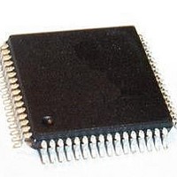
SAK-XC888CLM-8FFA 5V AC Infineon Technologies, SAK-XC888CLM-8FFA 5V AC Datasheet - Page 109

SAK-XC888CLM-8FFA 5V AC
Manufacturer Part Number
SAK-XC888CLM-8FFA 5V AC
Description
IC MCU 8BIT FLASH 64-LQFP
Manufacturer
Infineon Technologies
Series
XC8xxr
Datasheet
1.SAF-XC888CLM-6FFA_5V_AC.pdf
(144 pages)
Specifications of SAK-XC888CLM-8FFA 5V AC
Core Processor
XC800
Core Size
8-Bit
Speed
103.2MHz
Connectivity
CAN, LIN, SSI, UART/USART
Peripherals
Brown-out Detect/Reset, POR, PWM, WDT
Number Of I /o
48
Program Memory Size
32KB (32K x 8)
Program Memory Type
FLASH
Ram Size
1.75K x 8
Voltage - Supply (vcc/vdd)
4.5 V ~ 5.5 V
Data Converters
A/D 8x10b
Oscillator Type
Internal
Operating Temperature
-40°C ~ 125°C
Package / Case
64-LFQFP
Data Bus Width
8 bit
Data Ram Size
1.75 KB
Interface Type
UART, SSC
Maximum Clock Frequency
24 MHz
Number Of Programmable I/os
48
Number Of Timers
4
Operating Supply Voltage
5 V
Maximum Operating Temperature
+ 125 C
Mounting Style
SMD/SMT
Minimum Operating Temperature
- 40 C
On-chip Adc
10 bit, 8 Channel
For Use With
B158-H8743-X-X-7600IN - KIT STARTER XC886/888
Lead Free Status / RoHS Status
Lead free / RoHS Compliant
Eeprom Size
-
Lead Free Status / Rohs Status
Details
Other names
SP000210982
3.22
The On-Chip Debug Support (OCDS) provides the basic functionality required for the
software development and debugging of XC800-based systems.
The OCDS design is based on these principles:
•
•
•
•
Features
•
•
•
•
•
The OCDS functional blocks are shown in
block at the center of OCDS system brings together control signals and supports the
overall functionality. The MMC communicates with the XC800 Core, primarily via the
Debug Interface, and also receives reset and clock signals.
After processing memory address and control signals from the core, the MMC provides
proper access to the dedicated extra-memories: a Monitor ROM (holding the code) and
a Monitor RAM (for work-data and Monitor-stack).
The OCDS system is accessed through the JTAG
exclusively for testing and debugging activities and is not normally used in an
application. The dedicated MBC pin is used for external configuration and debugging
control.
Note: All the debug functionality described here can normally be used only after
1) The pins of the JTAG port can be assigned to either the primary port (Port 0) or either of the secondary ports
Data Sheet
(Ports 1 and 2/Port 5).
User must set the JTAG pins (TCK and TDI) as input during connection with the OCDS system.
Use the built-in debug functionality of the XC800 Core
Add a minimum of hardware overhead
Provide support for most of the operations by a Monitor Program
Use standard interfaces to communicate with the Host (a Debugger)
Set breakpoints on instruction address and on address range within the Program
Memory
Set breakpoints on internal RAM address range
Support unlimited software breakpoints in Flash/RAM code region
Process external breaks via JTAG and upon activating a dedicated pin
Step through the program code
XC886/888 has been started in OCDS mode.
On-Chip Debug Support
102
Figure
37. The Monitor Mode Control (MMC)
1)
, which is an interface dedicated
Functional Description
XC886/888CLM
V1.2, 2009-07


