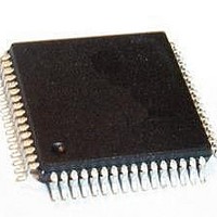
SAK-XC888CLM-8FFA 5V AC Infineon Technologies, SAK-XC888CLM-8FFA 5V AC Datasheet - Page 98

SAK-XC888CLM-8FFA 5V AC
Manufacturer Part Number
SAK-XC888CLM-8FFA 5V AC
Description
IC MCU 8BIT FLASH 64-LQFP
Manufacturer
Infineon Technologies
Series
XC8xxr
Datasheet
1.SAF-XC888CLM-6FFA_5V_AC.pdf
(144 pages)
Specifications of SAK-XC888CLM-8FFA 5V AC
Core Processor
XC800
Core Size
8-Bit
Speed
103.2MHz
Connectivity
CAN, LIN, SSI, UART/USART
Peripherals
Brown-out Detect/Reset, POR, PWM, WDT
Number Of I /o
48
Program Memory Size
32KB (32K x 8)
Program Memory Type
FLASH
Ram Size
1.75K x 8
Voltage - Supply (vcc/vdd)
4.5 V ~ 5.5 V
Data Converters
A/D 8x10b
Oscillator Type
Internal
Operating Temperature
-40°C ~ 125°C
Package / Case
64-LFQFP
Data Bus Width
8 bit
Data Ram Size
1.75 KB
Interface Type
UART, SSC
Maximum Clock Frequency
24 MHz
Number Of Programmable I/os
48
Number Of Timers
4
Operating Supply Voltage
5 V
Maximum Operating Temperature
+ 125 C
Mounting Style
SMD/SMT
Minimum Operating Temperature
- 40 C
On-chip Adc
10 bit, 8 Channel
For Use With
B158-H8743-X-X-7600IN - KIT STARTER XC886/888
Lead Free Status / RoHS Status
Lead free / RoHS Compliant
Eeprom Size
-
Lead Free Status / Rohs Status
Details
Other names
SP000210982
- Current page: 98 of 144
- Download datasheet (2Mb)
3.16
The High-Speed Synchronous Serial Interface (SSC) supports full-duplex and
half-duplex synchronous communication. The serial clock signal can be generated by
the SSC internally (master mode), using its own 16-bit baud-rate generator, or can be
received from an external master (slave mode). Data width, shift direction, clock polarity
and phase are programmable. This allows communication with SPI-compatible devices
or devices using other synchronous serial interfaces.
Features
•
•
•
•
•
•
Data is transmitted or received on lines TXD and RXD, which are normally connected to
the pins MTSR (Master Transmit/Slave Receive) and MRST (Master Receive/Slave
Transmit). The clock signal is output via line MS_CLK (Master Serial Shift Clock) or input
via line SS_CLK (Slave Serial Shift Clock). Both lines are normally connected to the pin
SCLK. Transmission and reception of data are double-buffered.
Figure 32
Data Sheet
Master and slave mode operation
– Full-duplex or half-duplex operation
Transmit and receive buffered
Flexible data format
– Programmable number of data bits: 2 to 8 bits
– Programmable shift direction: LSB or MSB shift first
– Programmable clock polarity: idle low or high state for the shift clock
– Programmable clock/data phase: data shift with leading or trailing edge of the shift
Variable baud rate
Compatible with Serial Peripheral Interface (SPI)
Interrupt generation
– On a transmitter empty condition
– On a receiver full condition
– On an error condition (receive, phase, baud rate, transmit error)
clock
shows the block diagram of the SSC.
High-Speed Synchronous Serial Interface
91
Functional Description
XC886/888CLM
V1.2, 2009-07
Related parts for SAK-XC888CLM-8FFA 5V AC
Image
Part Number
Description
Manufacturer
Datasheet
Request
R

Part Number:
Description:
IC MCU 8BIT FLASH 64-LQFP
Manufacturer:
Infineon Technologies
Datasheet:

Part Number:
Description:
IC MCU 8BIT FLASH 64-TQFP
Manufacturer:
Infineon Technologies
Datasheet:

Part Number:
Description:
High Performance 8-bit Microcontroller With On-chip Flash Memory And Can
Manufacturer:
Infineon Technologies Corporation
Datasheet:

Part Number:
Description:
IC MCU 8BIT FLASH TQFP-64
Manufacturer:
Infineon Technologies
Datasheet:

Part Number:
Description:
IC MCU 8BIT FLASH 64-LQFP
Manufacturer:
Infineon Technologies
Datasheet:

Part Number:
Description:
IC MCU 8BIT FLASH 64-LQFP
Manufacturer:
Infineon Technologies
Datasheet:

Part Number:
Description:
IC MCU 8BIT FLASH 64-LQFP
Manufacturer:
Infineon Technologies
Datasheet:

Part Number:
Description:
Manufacturer:
Infineon Technologies AG
Datasheet:

Part Number:
Description:
Manufacturer:
Infineon Technologies AG
Datasheet:

Part Number:
Description:
Manufacturer:
Infineon Technologies AG
Datasheet:

Part Number:
Description:
Manufacturer:
Infineon Technologies AG
Datasheet:

Part Number:
Description:
Manufacturer:
Infineon Technologies AG
Datasheet:

Part Number:
Description:
Manufacturer:
Infineon Technologies AG
Datasheet:

Part Number:
Description:
Manufacturer:
Infineon Technologies AG
Datasheet:

Part Number:
Description:
16-bit microcontroller with 2x2 KByte RAM
Manufacturer:
Infineon Technologies AG
Datasheet:


