C8051F023R Silicon Laboratories Inc, C8051F023R Datasheet - Page 13
C8051F023R
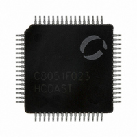
Manufacturer Part Number
C8051F023R
Description
IC 8051 MCU 64K FLASH 64TQFP
Manufacturer
Silicon Laboratories Inc
Series
C8051F02xr
Specifications of C8051F023R
Core Processor
8051
Core Size
8-Bit
Speed
25MHz
Connectivity
EBI/EMI, SMBus (2-Wire/I²C), SPI, UART/USART
Peripherals
Brown-out Detect/Reset, POR, PWM, Temp Sensor, WDT
Number Of I /o
32
Program Memory Size
64KB (64K x 8)
Program Memory Type
FLASH
Ram Size
4.25K x 8
Voltage - Supply (vcc/vdd)
2.7 V ~ 3.6 V
Data Converters
A/D 8x8b, 8x10b; D/A 2x12b
Oscillator Type
Internal
Operating Temperature
-40°C ~ 85°C
Package / Case
64-TQFP, 64-VQFP
Lead Free Status / RoHS Status
Contains lead / RoHS non-compliant
Eeprom Size
-
Other names
336-1035-2
Available stocks
Company
Part Number
Manufacturer
Quantity
Price
Company:

Part Number:
C8051F023R
Manufacturer:
Silicon Laboratories Inc
Quantity:
10 000


18. SYSTEM MANAGEMENT BUS / I2C BUS (SMBUS0) .................................................183
19. SERIAL PERIPHERAL INTERFACE BUS (SPI0) ........................................................197
20. UART0 ..................................................................................................................................205
21. UART1 ..................................................................................................................................215
Figure 18.1. SMBus0 Block Diagram ...................................................................................183
Figure 18.2. Typical SMBus Configuration ..........................................................................184
Figure 18.3. SMBus Transaction ...........................................................................................185
Figure 18.4. Typical Master Transmitter Sequence...............................................................187
Figure 18.5. Typical Master Receiver Sequence ...................................................................187
Figure 18.6. Typical Slave Transmitter Sequence .................................................................188
Figure 18.7. Typical Slave Receiver Sequence .....................................................................188
Figure 18.8. SMB0CN: SMBus0 Control Register ...............................................................191
Figure 18.9. SMB0CR: SMBus0 Clock Rate Register ..........................................................192
Figure 18.10. SMB0DAT: SMBus0 Data Register ...............................................................193
Figure 18.11. SMB0ADR: SMBus0 Address Register..........................................................193
Figure 18.12. SMB0STA: SMBus0 Status Register..............................................................194
Table 18.1. SMB0STA Status Codes and States ..................................................................195
Figure 19.1. SPI Block Diagram............................................................................................197
Figure 19.2. Typical SPI Interconnection..............................................................................198
Figure 19.3. Full Duplex Operation.......................................................................................199
Figure 19.4. Data/Clock Timing Diagram .............................................................................200
Figure 19.5. SPI0CFG: SPI0 Configuration Register............................................................201
Figure 19.6. SPI0CN: SPI0 Control Register ........................................................................202
Figure 19.7. SPI0CKR: SPI0 Clock Rate Register ................................................................203
Figure 19.8. SPI0DAT: SPI0 Data Register ..........................................................................203
Figure 20.1. UART0 Block Diagram.....................................................................................205
Table 20.1. UART0 Modes ..................................................................................................206
Figure 20.2. UART0 Mode 0 Interconnect............................................................................206
Figure 20.3. UART0 Mode 0 Timing Diagram .....................................................................206
Figure 20.4. UART0 Mode 1 Timing Diagram .....................................................................207
Figure 20.5. UART Modes 2 and 3 Timing Diagram............................................................208
Figure 20.6. UART Modes 1, 2, and 3 Interconnect Diagram ..............................................209
Figure 20.7. UART Multi-Processor Mode Interconnect Diagram .......................................210
Table 20.2. Oscillator Frequencies for Standard Baud Rates...............................................212
Figure 20.8. SCON0: UART0 Control Register....................................................................213
Figure 20.9. SBUF0: UART0 Data Buffer Register..............................................................214
Figure 20.10. SADDR0: UART0 Slave Address Register ....................................................214
Figure 20.11. SADEN0: UART0 Slave Address Enable Register ........................................214
Figure 21.1. UART1 Block Diagram.....................................................................................215
Table 21.1. UART1 Modes ..................................................................................................216
Figure 21.2. UART1 Mode 0 Interconnect............................................................................216
Figure 21.3. UART1 Mode 0 Timing Diagram .....................................................................216
Figure 21.4. UART1 Mode 1 Timing Diagram .....................................................................217
Figure 21.5. UART Modes 2 and 3 Timing Diagram............................................................218
Figure 21.6. UART Modes 1, 2, and 3 Interconnect Diagram ..............................................219
Rev. 1.4
C8051F020/1/2/3
13
Related parts for C8051F023R
Image
Part Number
Description
Manufacturer
Datasheet
Request
R

Part Number:
Description:
SMD/C°/SINGLE-ENDED OUTPUT SILICON OSCILLATOR
Manufacturer:
Silicon Laboratories Inc
Part Number:
Description:
Manufacturer:
Silicon Laboratories Inc
Datasheet:
Part Number:
Description:
N/A N/A/SI4010 AES KEYFOB DEMO WITH LCD RX
Manufacturer:
Silicon Laboratories Inc
Datasheet:
Part Number:
Description:
N/A N/A/SI4010 SIMPLIFIED KEY FOB DEMO WITH LED RX
Manufacturer:
Silicon Laboratories Inc
Datasheet:
Part Number:
Description:
N/A/-40 TO 85 OC/EZLINK MODULE; F930/4432 HIGH BAND (REV E/B1)
Manufacturer:
Silicon Laboratories Inc
Part Number:
Description:
EZLink Module; F930/4432 Low Band (rev e/B1)
Manufacturer:
Silicon Laboratories Inc
Part Number:
Description:
I°/4460 10 DBM RADIO TEST CARD 434 MHZ
Manufacturer:
Silicon Laboratories Inc
Part Number:
Description:
I°/4461 14 DBM RADIO TEST CARD 868 MHZ
Manufacturer:
Silicon Laboratories Inc
Part Number:
Description:
I°/4463 20 DBM RFSWITCH RADIO TEST CARD 460 MHZ
Manufacturer:
Silicon Laboratories Inc
Part Number:
Description:
I°/4463 20 DBM RADIO TEST CARD 868 MHZ
Manufacturer:
Silicon Laboratories Inc
Part Number:
Description:
I°/4463 27 DBM RADIO TEST CARD 868 MHZ
Manufacturer:
Silicon Laboratories Inc
Part Number:
Description:
I°/4463 SKYWORKS 30 DBM RADIO TEST CARD 915 MHZ
Manufacturer:
Silicon Laboratories Inc
Part Number:
Description:
N/A N/A/-40 TO 85 OC/4463 RFMD 30 DBM RADIO TEST CARD 915 MHZ
Manufacturer:
Silicon Laboratories Inc
Part Number:
Description:
I°/4463 20 DBM RADIO TEST CARD 169 MHZ
Manufacturer:
Silicon Laboratories Inc