C8051F023R Silicon Laboratories Inc, C8051F023R Datasheet - Page 33
C8051F023R
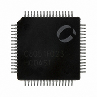
Manufacturer Part Number
C8051F023R
Description
IC 8051 MCU 64K FLASH 64TQFP
Manufacturer
Silicon Laboratories Inc
Series
C8051F02xr
Specifications of C8051F023R
Core Processor
8051
Core Size
8-Bit
Speed
25MHz
Connectivity
EBI/EMI, SMBus (2-Wire/I²C), SPI, UART/USART
Peripherals
Brown-out Detect/Reset, POR, PWM, Temp Sensor, WDT
Number Of I /o
32
Program Memory Size
64KB (64K x 8)
Program Memory Type
FLASH
Ram Size
4.25K x 8
Voltage - Supply (vcc/vdd)
2.7 V ~ 3.6 V
Data Converters
A/D 8x8b, 8x10b; D/A 2x12b
Oscillator Type
Internal
Operating Temperature
-40°C ~ 85°C
Package / Case
64-TQFP, 64-VQFP
Lead Free Status / RoHS Status
Contains lead / RoHS non-compliant
Eeprom Size
-
Other names
336-1035-2
Available stocks
Company
Part Number
Manufacturer
Quantity
Price
Company:

Part Number:
C8051F023R
Manufacturer:
Silicon Laboratories Inc
Quantity:
10 000


4.
MONEN
VREFD
XTAL1
XTAL2
VREFA
VREF0
VREF1
DGND
AGND
Name
VREF
VDD
/RST
TMS
TCK
TDO
AV+
TDI
PINOUT AND PACKAGE DEFINITIONS
37, 64,
38, 63,
11, 14
10, 13
F020
F022
Pin Numbers
90
89
26
27
28
12
16
17
15
1
2
3
4
5
24, 41,
25, 40,
F021
F023
57
56
58
59
60
61
62
17
18
19
6
5
7
8
D Out JTAG Test Data Output with internal pull-up. Data is shifted out on
A Out Crystal Output. This pin is the excitation driver for a crystal or
D I/O Device Reset. Open-drain output of internal VDD monitor. Is driven
A I/O Bandgap Voltage Reference Output (all devices).
Type
D In
D In
D In
A In
D In
A In
A In
A In
A In
Table 4.1. Pin Definitions
Description
Digital Supply Voltage. Must be tied to +2.7 to +3.6 V.
Digital Ground. Must be tied to Ground.
Analog Supply Voltage. Must be tied to +2.7 to +3.6 V.
Analog Ground. Must be tied to Ground.
JTAG Test Mode Select with internal pull-up.
JTAG Test Clock with internal pull-up.
JTAG Test Data Input with internal pull-up. TDI is latched on the
rising edge of TCK.
TDO on the falling edge of TCK. TDO output is a tri-state driver.
low when VDD is <2.7 V and MONEN is high. An external source
can initiate a system reset by driving this pin low.
Crystal Input. This pin is the return for the internal oscillator circuit
for a crystal or ceramic resonator. For a precision internal clock,
connect a crystal or ceramic resonator from XTAL1 to XTAL2. If
overdriven by an external CMOS clock, this becomes the system
clock.
ceramic resonator.
VDD Monitor Enable. When tied high, this pin enables the internal
VDD monitor, which forces a system reset when VDD is < 2.7 V.
When tied low, the internal VDD monitor is disabled.
DAC Voltage Reference Input (F021/3 only).
ADC0 and ADC1 Voltage Reference Input.
ADC0 Voltage Reference Input.
ADC1 Voltage Reference Input.
DAC Voltage Reference Input.
Rev. 1.4
C8051F020/1/2/3
33
Related parts for C8051F023R
Image
Part Number
Description
Manufacturer
Datasheet
Request
R

Part Number:
Description:
SMD/C°/SINGLE-ENDED OUTPUT SILICON OSCILLATOR
Manufacturer:
Silicon Laboratories Inc
Part Number:
Description:
Manufacturer:
Silicon Laboratories Inc
Datasheet:
Part Number:
Description:
N/A N/A/SI4010 AES KEYFOB DEMO WITH LCD RX
Manufacturer:
Silicon Laboratories Inc
Datasheet:
Part Number:
Description:
N/A N/A/SI4010 SIMPLIFIED KEY FOB DEMO WITH LED RX
Manufacturer:
Silicon Laboratories Inc
Datasheet:
Part Number:
Description:
N/A/-40 TO 85 OC/EZLINK MODULE; F930/4432 HIGH BAND (REV E/B1)
Manufacturer:
Silicon Laboratories Inc
Part Number:
Description:
EZLink Module; F930/4432 Low Band (rev e/B1)
Manufacturer:
Silicon Laboratories Inc
Part Number:
Description:
I°/4460 10 DBM RADIO TEST CARD 434 MHZ
Manufacturer:
Silicon Laboratories Inc
Part Number:
Description:
I°/4461 14 DBM RADIO TEST CARD 868 MHZ
Manufacturer:
Silicon Laboratories Inc
Part Number:
Description:
I°/4463 20 DBM RFSWITCH RADIO TEST CARD 460 MHZ
Manufacturer:
Silicon Laboratories Inc
Part Number:
Description:
I°/4463 20 DBM RADIO TEST CARD 868 MHZ
Manufacturer:
Silicon Laboratories Inc
Part Number:
Description:
I°/4463 27 DBM RADIO TEST CARD 868 MHZ
Manufacturer:
Silicon Laboratories Inc
Part Number:
Description:
I°/4463 SKYWORKS 30 DBM RADIO TEST CARD 915 MHZ
Manufacturer:
Silicon Laboratories Inc
Part Number:
Description:
N/A N/A/-40 TO 85 OC/4463 RFMD 30 DBM RADIO TEST CARD 915 MHZ
Manufacturer:
Silicon Laboratories Inc
Part Number:
Description:
I°/4463 20 DBM RADIO TEST CARD 169 MHZ
Manufacturer:
Silicon Laboratories Inc