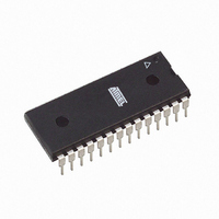
ATMEGA88-20PU Atmel, ATMEGA88-20PU Datasheet - Page 23

ATMEGA88-20PU
Manufacturer Part Number
ATMEGA88-20PU
Description
IC AVR MCU 8K 20MHZ 5V 28DIP
Manufacturer
Atmel
Series
AVR® ATmegar
Specifications of ATMEGA88-20PU
Core Processor
AVR
Core Size
8-Bit
Speed
20MHz
Connectivity
I²C, SPI, UART/USART
Peripherals
Brown-out Detect/Reset, POR, PWM, WDT
Number Of I /o
23
Program Memory Size
8KB (4K x 16)
Program Memory Type
FLASH
Eeprom Size
512 x 8
Ram Size
1K x 8
Voltage - Supply (vcc/vdd)
2.7 V ~ 5.5 V
Data Converters
A/D 6x10b
Oscillator Type
Internal
Operating Temperature
-40°C ~ 85°C
Package / Case
28-DIP (0.300", 7.62mm)
Cpu Family
ATmega
Device Core
AVR
Device Core Size
8b
Frequency (max)
20MHz
Interface Type
SPI/TWI/USART
Total Internal Ram Size
1KB
# I/os (max)
23
Number Of Timers - General Purpose
3
Operating Supply Voltage (typ)
3.3/5V
Operating Supply Voltage (max)
5.5V
Operating Supply Voltage (min)
2.7V
On-chip Adc
6-chx10-bit
Instruction Set Architecture
RISC
Operating Temp Range
-40C to 85C
Operating Temperature Classification
Industrial
Mounting
Through Hole
Pin Count
28
Package Type
PDIP
Processor Series
ATMEGA8x
Core
AVR8
Data Bus Width
8 bit
Data Ram Size
1 KB
Maximum Clock Frequency
20 MHz
Number Of Programmable I/os
23
Number Of Timers
3
Operating Supply Voltage
2.7 V to 5.5 V
Maximum Operating Temperature
+ 85 C
Mounting Style
Through Hole
3rd Party Development Tools
EWAVR, EWAVR-BL
Development Tools By Supplier
ATAVRDRAGON, ATSTK500, ATSTK600, ATAVRISP2, ATAVRONEKIT, ATAVRTS2080A, ATASTK512-EK1-IND
Minimum Operating Temperature
- 40 C
Package
28PDIP
Family Name
ATmega
Maximum Speed
20 MHz
For Use With
ATAVRDRAGON - KIT DRAGON 32KB FLASH MEM AVRATAVRISP2 - PROGRAMMER AVR IN SYSTEM
Lead Free Status / RoHS Status
Lead free / RoHS Compliant
- Current page: 23 of 378
- Download datasheet (8Mb)
2545S–AVR–07/10
When the write access time has elapsed, the EEPE bit is cleared by hardware. The user soft-
ware can poll this bit and wait for a zero before writing the next byte. When EEPE has been set,
the CPU is halted for two cycles before the next instruction is executed.
• Bit 0 – EERE: EEPROM Read Enable
The EEPROM Read Enable Signal EERE is the read strobe to the EEPROM. When the correct
address is set up in the EEAR Register, the EERE bit must be written to a logic one to trigger the
EEPROM read. The EEPROM read access takes one instruction, and the requested data is
available immediately. When the EEPROM is read, the CPU is halted for four cycles before the
next instruction is executed.
The user should poll the EEPE bit before starting the read operation. If a write operation is in
progress, it is neither possible to read the EEPROM, nor to change the EEAR Register.
The calibrated Oscillator is used to time the EEPROM accesses.
gramming time for EEPROM access from the CPU.
Table 7-2.
The following code examples show one assembly and one C function for writing to the
EEPROM. The examples assume that interrupts are controlled (for example by disabling inter-
rupts globally) so that no interrupts will occur during execution of these functions. The examples
also assume that no Flash Boot Loader is present in the software. If such code is present, the
EEPROM write function must also wait for any ongoing SPM command to finish.
Symbol
EEPROM write
(from CPU)
EEPROM Programming Time
Number of Calibrated RC Oscillator Cycles
26,368
ATmega48/88/168
Table 7-2
Typ Programming Time
lists the typical pro-
3.3 ms
23
Related parts for ATMEGA88-20PU
Image
Part Number
Description
Manufacturer
Datasheet
Request
R

Part Number:
Description:
IC MCU AVR 8K 5V 20MHZ 32-TQFP
Manufacturer:
Atmel
Datasheet:

Part Number:
Description:
Manufacturer:
Atmel Corporation
Datasheet:

Part Number:
Description:
Manufacturer:
Atmel Corporation
Datasheet:

Part Number:
Description:
MCU AVR 8K FLASH 15MHZ 32-QFN
Manufacturer:
Atmel
Datasheet:

Part Number:
Description:
IC AVR MCU 8K 20MHZ 5V 32TQFP
Manufacturer:
Atmel
Datasheet:

Part Number:
Description:
IC AVR MCU 8K 20MHZ 5V 32-QFN
Manufacturer:
Atmel
Datasheet:

Part Number:
Description:
IC MCU AVR 8K 5V 20MHZ 32-TQFP
Manufacturer:
Atmel
Datasheet:

Part Number:
Description:
IC MCU AVR 8K 5V 20MHZ 32-QFN
Manufacturer:
Atmel
Datasheet:

Part Number:
Description:
IC MCU AVR 8K 5V 20MHZ 32-QFN
Manufacturer:
Atmel
Datasheet:

Part Number:
Description:
IC MCU AVR 8K 5V 20MHZ 28-DIP
Manufacturer:
Atmel
Datasheet:

Part Number:
Description:
IC MCU AVR 8K 5V 20MHZ 28-DIP
Manufacturer:
Atmel
Datasheet:

Part Number:
Description:
MCU AVR 8K FLASH 20MHZ 32TQFP
Manufacturer:
Atmel
Datasheet:

Part Number:
Description:
MCU AVR 8K FLASH 20MHZ 32QFN
Manufacturer:
Atmel
Datasheet:


