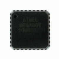
ATMEGA88V-10MU Atmel, ATMEGA88V-10MU Datasheet - Page 76

ATMEGA88V-10MU
Manufacturer Part Number
ATMEGA88V-10MU
Description
IC AVR MCU 8K 10MHZ 1.8V 32-QFN
Manufacturer
Atmel
Series
AVR® ATmegar
Specifications of ATMEGA88V-10MU
Core Processor
AVR
Core Size
8-Bit
Speed
10MHz
Connectivity
I²C, SPI, UART/USART
Peripherals
Brown-out Detect/Reset, POR, PWM, WDT
Number Of I /o
23
Program Memory Size
8KB (4K x 16)
Program Memory Type
FLASH
Eeprom Size
512 x 8
Ram Size
1K x 8
Voltage - Supply (vcc/vdd)
1.8 V ~ 5.5 V
Data Converters
A/D 8x10b
Oscillator Type
Internal
Operating Temperature
-40°C ~ 85°C
Package / Case
32-VQFN Exposed Pad, 32-HVQFN, 32-SQFN, 32-DHVQFN
Processor Series
ATMEGA8x
Core
AVR8
Data Bus Width
8 bit
Data Ram Size
1 KB
Interface Type
2-Wire, SPI, USART, Serial
Maximum Clock Frequency
20 MHz
Number Of Programmable I/os
23
Number Of Timers
3 bit
Operating Supply Voltage
1.8 V to 5.5 V
Maximum Operating Temperature
+ 85 C
Mounting Style
SMD/SMT
3rd Party Development Tools
EWAVR, EWAVR-BL
Minimum Operating Temperature
- 40 C
On-chip Adc
10 bit, 8 Channel
Controller Family/series
AVR MEGA
No. Of I/o's
23
Eeprom Memory Size
512Byte
Ram Memory Size
1KB
Cpu Speed
10MHz
No. Of Timers
3
Rohs Compliant
Yes
Package
32MLF EP
Device Core
AVR
Family Name
ATmega
Maximum Speed
10 MHz
For Use With
ATAVRDRAGON - KIT DRAGON 32KB FLASH MEM AVRATAVRISP2 - PROGRAMMER AVR IN SYSTEM
Lead Free Status / RoHS Status
Lead free / RoHS Compliant
Available stocks
Company
Part Number
Manufacturer
Quantity
Price
Company:
Part Number:
ATMEGA88V-10MU
Manufacturer:
ATMEL
Quantity:
2 100
Part Number:
ATMEGA88V-10MU
Manufacturer:
ATMEL/爱特梅尔
Quantity:
20 000
Company:
Part Number:
ATMEGA88V-10MUR
Manufacturer:
Atmel
Quantity:
6 000
- Current page: 76 of 378
- Download datasheet (8Mb)
76
ATmega48/88/168
Table 13-2
ure 13-5
in the modules having the alternate function.
Table 13-2.
The following subsections shortly describe the alternate functions for each port, and relate the
overriding signals to the alternate function. Refer to the alternate function description for further
details.
Signal Name
PUOE
PUOV
DDOE
DDOV
PVOE
PVOV
PTOE
DIEOE
DIEOV
DI
AIO
are not shown in the succeeding tables. The overriding signals are generated internally
summarizes the function of the overriding signals. The pin and port indexes from
Generic Description of Overriding Signals for Alternate Functions
Full Name
Pull-up Override
Enable
Pull-up Override
Value
Data Direction
Override Enable
Data Direction
Override Value
Port Value
Override Enable
Port Value
Override Value
Port Toggle
Override Enable
Digital Input
Enable Override
Enable
Digital Input
Enable Override
Value
Digital Input
Analog
Input/Output
Description
If this signal is set, the pull-up enable is controlled by the PUOV
signal. If this signal is cleared, the pull-up is enabled when
{DDxn, PORTxn, PUD} = 0b010.
If PUOE is set, the pull-up is enabled/disabled when PUOV is
set/cleared, regardless of the setting of the DDxn, PORTxn,
and PUD Register bits.
If this signal is set, the Output Driver Enable is controlled by the
DDOV signal. If this signal is cleared, the Output driver is
enabled by the DDxn Register bit.
If DDOE is set, the Output Driver is enabled/disabled when
DDOV is set/cleared, regardless of the setting of the DDxn
Register bit.
If this signal is set and the Output Driver is enabled, the port
value is controlled by the PVOV signal. If PVOE is cleared, and
the Output Driver is enabled, the port Value is controlled by the
PORTxn Register bit.
If PVOE is set, the port value is set to PVOV, regardless of the
setting of the PORTxn Register bit.
If PTOE is set, the PORTxn Register bit is inverted.
If this bit is set, the Digital Input Enable is controlled by the
DIEOV signal. If this signal is cleared, the Digital Input Enable
is determined by MCU state (Normal mode, sleep mode).
If DIEOE is set, the Digital Input is enabled/disabled when
DIEOV is set/cleared, regardless of the MCU state (Normal
mode, sleep mode).
This is the Digital Input to alternate functions. In the figure, the
signal is connected to the output of the Schmitt Trigger but
before the synchronizer. Unless the Digital Input is used as a
clock source, the module with the alternate function will use its
own synchronizer.
This is the Analog Input/output to/from alternate functions. The
signal is connected directly to the pad, and can be used bi-
directionally.
2545S–AVR–07/10
Fig-
Related parts for ATMEGA88V-10MU
Image
Part Number
Description
Manufacturer
Datasheet
Request
R

Part Number:
Description:
IC MCU AVR 8K 5V 10MHZ 32-TQFP
Manufacturer:
Atmel
Datasheet:

Part Number:
Description:
IC AVR MCU 8K 10MHZ 1.8V 32TQFP
Manufacturer:
Atmel
Datasheet:

Part Number:
Description:
IC MCU AVR 8K 5V 10MHZ 32-TQFP
Manufacturer:
Atmel
Datasheet:

Part Number:
Description:
IC MCU AVR 8K 5V 10MHZ 32-QFN
Manufacturer:
Atmel
Datasheet:

Part Number:
Description:
IC MCU AVR 8K 5V 10MHZ 32-QFN
Manufacturer:
Atmel
Datasheet:

Part Number:
Description:
IC MCU AVR 8K 5V 10MHZ 28-DIP
Manufacturer:
Atmel
Datasheet:

Part Number:
Description:
IC MCU AVR 8K 5V 10MHZ 28-DIP
Manufacturer:
Atmel
Datasheet:

Part Number:
Description:
MCU AVR 8K FLASH 10MHZ 32TQFP
Manufacturer:
Atmel
Datasheet:

Part Number:
Description:
MCU AVR 8K FLASH 10MHZ 32QFN
Manufacturer:
Atmel
Datasheet:

Part Number:
Description:
IC AVR MCU 8K 10MHZ 1.8V 28DIP
Manufacturer:
Atmel
Datasheet:

Part Number:
Description:
IC MCU AVR 8K 5V 20MHZ 32-TQFP
Manufacturer:
Atmel
Datasheet:

Part Number:
Description:
Manufacturer:
Atmel Corporation
Datasheet:


