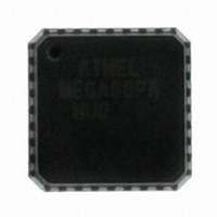
ATMEGA88PA-MU Atmel, ATMEGA88PA-MU Datasheet - Page 83

ATMEGA88PA-MU
Manufacturer Part Number
ATMEGA88PA-MU
Description
MCU AVR 8K ISP FLASH MEM 32-QFN
Manufacturer
Atmel
Series
AVR® ATmegar
Datasheets
1.ATMEGA48A-PU.pdf
(566 pages)
2.ATMEGA48A-PU.pdf
(33 pages)
3.ATMEGA48PA-MMH.pdf
(26 pages)
Specifications of ATMEGA88PA-MU
Core Processor
AVR
Core Size
8-Bit
Speed
20MHz
Connectivity
I²C, SPI, UART/USART
Peripherals
Brown-out Detect/Reset, POR, PWM, WDT
Number Of I /o
23
Program Memory Size
8KB (4K x 16)
Program Memory Type
FLASH
Eeprom Size
512 x 8
Ram Size
1K x 8
Voltage - Supply (vcc/vdd)
1.8 V ~ 5.5 V
Data Converters
A/D 8x10b
Oscillator Type
Internal
Operating Temperature
-40°C ~ 85°C
Package / Case
32-VQFN Exposed Pad, 32-HVQFN, 32-SQFN, 32-DHVQFN
Controller Family/series
AVR MEGA
No. Of I/o's
23
Eeprom Memory Size
512Byte
Ram Memory Size
1KB
Cpu Speed
20MHz
No. Of Timers
3
Rohs Compliant
Yes
Package
32QFN EP
Device Core
AVR
Family Name
ATmega
Maximum Speed
20 MHz
Operating Supply Voltage
2.5|3.3|5 V
Data Bus Width
8 Bit
Number Of Programmable I/os
23
Interface Type
SPI/TWI/USART
On-chip Adc
8-chx10-bit
Number Of Timers
3
For Use With
ATSTK600-TQFP32 - STK600 SOCKET/ADAPTER 32-TQFPATSTK600-DIP40 - STK600 SOCKET/ADAPTER 40-PDIP770-1007 - ISP 4PORT ATMEL AVR MCU SPI/JTAGATAVRDRAGON - KIT DRAGON 32KB FLASH MEM AVRATAVRISP2 - PROGRAMMER AVR IN SYSTEMATJTAGICE2 - AVR ON-CHIP D-BUG SYSTEM
Lead Free Status / RoHS Status
Lead free / RoHS Compliant
Available stocks
Company
Part Number
Manufacturer
Quantity
Price
Part Number:
ATMEGA88PA-MU
Manufacturer:
MICROCHIP/微芯
Quantity:
20 000
- Current page: 83 of 566
- Download datasheet (23Mb)
13.3.1
8271C–AVR–08/10
Alternate Functions of Port B
The Port B pins with alternate functions are shown in
Table 13-3.
The alternate pin configuration is as follows:
• XTAL2/TOSC2/PCINT7 – Port B, Bit 7
XTAL2: Chip clock Oscillator pin 2. Used as clock pin for crystal Oscillator or Low-frequency
crystal Oscillator. When used as a clock pin, the pin can not be used as an I/O pin.
TOSC2: Timer Oscillator pin 2. Used only if internal calibrated RC Oscillator is selected as chip
clock source, and the asynchronous timer is enabled by the correct setting in ASSR. When the
AS2 bit in ASSR is set (one) and the EXCLK bit is cleared (zero) to enable asynchronous clock-
ing of Timer/Counter2 using the Crystal Oscillator, pin PB7 is disconnected from the port, and
becomes the inverting output of the Oscillator amplifier. In this mode, a crystal Oscillator is con-
nected to this pin, and the pin cannot be used as an I/O pin.
PCINT7: Pin Change Interrupt source 7. The PB7 pin can serve as an external interrupt source.
If PB7 is used as a clock pin, DDB7, PORTB7 and PINB7 will all read 0.
• XTAL1/TOSC1/PCINT6 – Port B, Bit 6
XTAL1: Chip clock Oscillator pin 1. Used for all chip clock sources except internal calibrated RC
Oscillator. When used as a clock pin, the pin can not be used as an I/O pin.
TOSC1: Timer Oscillator pin 1. Used only if internal calibrated RC Oscillator is selected as chip
clock source, and the asynchronous timer is enabled by the correct setting in ASSR. When the
ATmega48A/48PA/88A/88PA/168A/168PA/328/328
Port Pin
PB7
PB6
PB5
PB4
PB3
PB2
PB1
PB0
Port B Pins Alternate Functions
Alternate Functions
XTAL2 (
TOSC2 (
PCINT7 (Pin Change Interrupt 7)
XTAL1 (
TOSC1 (
PCINT6 (Pin Change Interrupt 6)
SCK (SPI Bus Master clock Input)
PCINT5 (Pin Change Interrupt 5)
MISO (SPI Bus Master Input/Slave Output)
PCINT4 (Pin Change Interrupt 4)
MOSI (SPI Bus Master Output/Slave Input)
OC2A (Timer/Counter2 Output Compare Match A Output)
PCINT3 (Pin Change Interrupt 3)
SS (SPI Bus Master Slave select)
OC1B (Timer/Counter1 Output Compare Match B Output)
PCINT2 (Pin Change Interrupt 2)
OC1A (Timer/Counter1 Output Compare Match A Output)
PCINT1 (Pin Change Interrupt 1)
ICP1 (Timer/Counter1 Input Capture Input)
CLKO (Divided System Clock Output)
PCINT0 (Pin Change Interrupt 0)
Chip Clock Oscillator pin 2
Chip Clock Oscillator pin 1 or External clock input
Timer Oscillator pin 2
Timer Oscillator pin 1
)
)
)
Table
13-3.
)
83
Related parts for ATMEGA88PA-MU
Image
Part Number
Description
Manufacturer
Datasheet
Request
R

Part Number:
Description:
IC MCU AVR 8K 5V 20MHZ 32-TQFP
Manufacturer:
Atmel
Datasheet:

Part Number:
Description:
Manufacturer:
Atmel Corporation
Datasheet:

Part Number:
Description:
Manufacturer:
Atmel Corporation
Datasheet:

Part Number:
Description:
MCU AVR 8K FLASH 15MHZ 32-QFN
Manufacturer:
Atmel
Datasheet:

Part Number:
Description:
IC AVR MCU 8K 20MHZ 5V 32TQFP
Manufacturer:
Atmel
Datasheet:

Part Number:
Description:
IC AVR MCU 8K 20MHZ 5V 32-QFN
Manufacturer:
Atmel
Datasheet:

Part Number:
Description:
IC AVR MCU 8K 20MHZ 5V 28DIP
Manufacturer:
Atmel
Datasheet:

Part Number:
Description:
IC MCU AVR 8K 5V 20MHZ 32-TQFP
Manufacturer:
Atmel
Datasheet:

Part Number:
Description:
IC MCU AVR 8K 5V 20MHZ 32-QFN
Manufacturer:
Atmel
Datasheet:

Part Number:
Description:
IC MCU AVR 8K 5V 20MHZ 32-QFN
Manufacturer:
Atmel
Datasheet:

Part Number:
Description:
IC MCU AVR 8K 5V 20MHZ 28-DIP
Manufacturer:
Atmel
Datasheet:

Part Number:
Description:
IC MCU AVR 8K 5V 20MHZ 28-DIP
Manufacturer:
Atmel
Datasheet:

Part Number:
Description:
MCU AVR 8K FLASH 20MHZ 32TQFP
Manufacturer:
Atmel
Datasheet:


