Z32AN00NW200SG Zilog, Z32AN00NW200SG Datasheet
Z32AN00NW200SG
Specifications of Z32AN00NW200SG
Available stocks


Related parts for Z32AN00NW200SG


Z32AN00NW200SG Summary of contents
Page 1
... Encore! 32™ Series Microcontroller (Z32AN) High Performance ARM9 SoC Data Sheet DS0200-003 Copyright ©2009 by Zilog, Inc. All Rights Reserved www.zilog.com ...
Page 2
... OTHERWISE. The information contained within this document has been verified according to the general principles of electrical and mechanical engineering. TM Encore trademark of Zilog, Inc. ARM® and Thumb® are registered trademarks of ARM Limited in the European Union and other countries. All other product or service names are the property of their respective owners. ...
Page 3
Revision History Each instance in the revision history reflects a change to this document from its previous revision. For more details, refer to the corresponding pages and appropriate links in the table below. Date August 2008 September 23, 2008 February ...
Page 4
Z32AN Series Data Sheet The Z32AN Series is a highly integrated System-on-Chip (SoC) based on the ARM922T core. Available in a 256-BGA package, the Z32AN Series provides a rich set of features on a single chip and enables designers to ...
Page 5
Z32AN Series Data Sheet Chapter 1: Pin Description ............................................................................................. 1 1.1 System Pins ............................................................................................................................................. 1 1.2 External Bus Interface........................................................................................................................... 1 1.3 Secondary External Bus Interface ...................................................................................................... 1 1.4 External DMA Interface........................................................................................................................ 2 1.5 Timer/Counter........................................................................................................................................ 2 1.6 RTC........................................................................................................................................................... 2 1.7 UARTs ...
Page 6
Z32AN Series Data Sheet 5.2 Accesses............................................................................................................................................... 18 5.3 Restricted / Reserved Addresses...................................................................................................... 18 5.4 ROM/SRAM Remapping .................................................................................................................... 18 5.5 Internal SRAM....................................................................................................................................... 18 5.5.1 Clock Disable....................................................................................................................18 5.5.2 Zeroization .........................................................................................................................18 5.5.3 Address FFFF8068h: INT_SRAM_CLR – Internal SRAM Clear Register ............................18 5.6 Internal ...
Page 7
Z32AN Series Data Sheet Chapter 8: DMA Controller........................................................................................... 49 8.1 Channel Arbitration and Bursts......................................................................................................... 49 8.2 DMA Source and Destination Addressing ...................................................................................... 50 8.3 Data Movement from the DMA FIFO to the Destination ............................................................. 51 8.4 Memory Buffer Alignment ................................................................................................................. ...
Page 8
Z32AN Series Data Sheet Chapter 11: Real-Time Clock (RTC) ............................................................................ 93 11.1 Real-Time Clock Time/Counter Registers........................................................................................ 93 11.2 RTC Alarm............................................................................................................................................. 93 11.3 RTC Wake ............................................................................................................................................. 93 11.4 RTC Oscillator Source ......................................................................................................................... 93 11.5 RTC Battery Backup............................................................................................................................ 93 11.6 RTC Reset.............................................................................................................................................. ...
Page 9
Z32AN Series Data Sheet 15.5.3 Offset 008h: LCD_WR – LCD Write Register ..................................................................112 Chapter 16: Timers ...................................................................................................... 113 16.1 Watchdog Timer (WDT).................................................................................................................... 113 16.1.1 Enabling...........................................................................................................................113 16.1.2 Time Delay Period Selection..........................................................................................113 16.1.3 Registers (Base → FFFEC000h) .......................................................................................114 16.2 16-bit PWM Timers ...
Page 10
Z32AN Series Data Sheet 18.6 Error Detection................................................................................................................................... 148 18.6.1 Transmit Overrun.............................................................................................................148 18.6.2 Mode Fault (Multi-Master Collision) ..............................................................................148 18.6.3 Slave Mode Abort ..........................................................................................................148 18.6.4 Receive Overrun ............................................................................................................148 18.7 SPI Interrupts ....................................................................................................................................... 148 18.8 SPI Baud Rate Generator (BRG)..................................................................................................... 149 18.9 SPI ...
Page 11
Z32AN Series Data Sheet 20.3 Registers (Base: GPIO0→FFFF5000h, GPIO1→FFFF6000h, GPIO2→FFFF7000h) ....................... 175 20.4 Using Output ...................................................................................................................................... 176 20.5 Configuring Interrupts....................................................................................................................... 176 20.6 Handling Interrupts............................................................................................................................ 176 20.7 Wake Function .................................................................................................................................. 176 Chapter 21: Electrical Characteristics ...................................................................... 177 21.1 Absolute Maximum Ratings ...
Page 12
Z32AN Series Data Sheet Figure 2-1: Reset Module Block Diagram......................................................................................................... 7 Figure 3-1: Simplified PMU Block Diagram ....................................................................................................... 8 Figure 3-2: Main Crystal External Circuits ....................................................................................................... 10 Figure 3-3: System Clocking ............................................................................................................................. 10 Figure 7-1: CS1 as A[24] .................................................................................................................................... 30 ...
Page 13
Z32AN Series Data Sheet Table 3-1: PMU Module Inputs and Outputs ................................................................................................... 8 Table 6-1: Interrupt Source to Channel Mapping ........................................................................................ 21 Table 7-1: Pin Functions vs. Control Style ....................................................................................................... 29 Table 7-2: Single Read/Write Timing (based on MEMC_TIMN)................................................................... 31 ...
Page 14
Z32AN Series Data Sheet Chapter 1: Pin Description 1.1 System Pins Pin Name Dir Function nRSTIN I System Reset: Schmitt trigger input. nRSTOUT O Reset Out: 4mA drive. CLKXI I System Clock Oscillator Input CLKXO O System Clock Oscillator Output ...
Page 15
Z32AN Series Data Sheet 1.4 External DMA Interface After reset, all external DMA interface pins default to GPIO. Pin Name Dir Function External DMA Transmit Request: Schmitt trigger input. 4mA drive. Multiplexed TxREQ I with GPIO_2[8]. External DMA Transmit Acknowledge: ...
Page 16
Z32AN Series Data Sheet 1.7.3 UART2 Pin Name Type Function RxD[2] I UART2 Data Input: 5V tolerant. 4mA drive. Multiplexed with GPIO_0[31]. TxD[2] O UART2 Data Output: 5V tolerant. 4mA drive. Multiplexed with GPIO_1[0]. nCTS[2] I UART2 Clear to Send: ...
Page 17
Z32AN Series Data Sheet 1.10 SmartCard Interface All SmartCard pins default to GPIOs at reset. 1.10.1 Port 0 Pin Name Type Function SC_CLK[0] O SmartCard Port 0 Clock: 4mA drive. Multiplexed with GPIO_1[19]. SC_IO[0] I/O SmartCard Port 0 I/O: Internal ...
Page 18
Z32AN Series Data Sheet 1.14 Magnetic Card Reader Pin Name Type Function MCR_P[2:0] AI Memory Card Reader Positive Analog Inputs: MCR_N[2:0] AI Memory Card Reader Negative Analog Inputs: MCR_VREF A Memory Card Voltage Reference: Connect external 100nF (ceramic) to ground. ...
Page 19
Z32AN Series Data Sheet 1.17 Pin Assignments, 256 BGA Package AVSS_ AVSS_ MISO[0] MOSI[0] SCK[0] A ADC USB AVDD_ AVDD_ nSS[0] MISO[1] SCK[1] B ADC USB ADC_ ADC_ nCS[9] nOE MOSI[1] C IN[2] IN{1] ADC_ nCS[8] ...
Page 20
Z32AN Series Data Sheet Chapter 2: Reset The Z32AN Series provides 3 types of reset operations: System Reset, Hard Reset, and Peripheral Reset 2.1 System Reset A system reset is caused by a Hard Reset or a Soft Reset. A ...
Page 21
Z32AN Series Data Sheet Chapter 3: System Clocks and Power Management The Z32AN Series contains a Power Management Unit (PMU) that controls system clocking and power management. The configuration of the PMU is performed through the PMU registers. Upon a ...
Page 22
Z32AN Series Data Sheet 3.1 Power Modes Mode Initiation HALT ARM922T CP15 of ARM922T Wait-for-IRQ PMU_CFG and IDLE PMU_CLK_EN STOP PMU_CFG Battery Back Automatic when Up power is removed 3.1.1 HALT - ARM922 Wait for Interrupt This is an intrinsic ...
Page 23
Z32AN Series Data Sheet USB Wake: USB can return the SoC to active operation from Idle or Stop Modes. The lowest power for USB suspend is achieved through “stop” mode. The PMU can be configured to wake when USB ...
Page 24
Z32AN Series Data Sheet 3.5 PMU Registers: (Base → FFFFE000h) The PMU registers are reset by a hard reset, unless otherwise noted in the register description. Most of the system and registers are reset by a system reset, but the ...
Page 25
Z32AN Series Data Sheet 3.5.2 Offset 004h: PMUCLK – PMU Clock Control Register Bits Type Reset 29: 23: 15:08 RW 00h 07: ...
Page 26
Z32AN Series Data Sheet 3.5.3 Offset 008h: PMUCKEN – PMU Clock Enable Register Bits Type Reset RW ...
Page 27
Z32AN Series Data Sheet 3.5.4 Offset 00Ch: PMURESET – PMU Reset Register Bits Type Reset 31: 15: RW1C ...
Page 28
Z32AN Series Data Sheet 3.5.6 Offset 01Ch: PMUCFG – PMU Configuration Register Bits Type Reset 29:27 RW 000 21:19 ...
Page 29
Z32AN Series Data Sheet Chapter 4: ARM922T Core and Embedded ICE The ARM922T core of the Z32AN Series contains a JTAG interface and an embedded In-Circuit Emulator (ICE) interface. For more details on these features, refer to the ARM922T Technical ...
Page 30
Z32AN Series Data Sheet Chapter 5: Memory Organization 5.1 Memory Map FFFFFFFFh APB Peripherals 256 KB FFFC0000h FFFBFFFFh AHB Peripherals 64 KB FFFA0000h FFF9FFFFh Restricted 60000000h 5FFFFFFFh External SDRAM 512 MB Primary bus 40000000h 3FFFFFFFh External SDRAM 512 MB Secondary ...
Page 31
Z32AN Series Data Sheet REMAP=0 REMAP=1 5.2 Accesses All AHB devices can be accessed with byte, halfword or word accesses. APB devices can be read as bytes or halfwords, but should only be written with word accesses. Byte or halfword ...
Page 32
Z32AN Series Data Sheet 5.6 Internal ROM and Boot Program After reset, the ARM CPU begins executing code out of the internal ROM at address 0h. 5.6.1 Boot locations After reset, boot code will search both the primary secondary busses ...
Page 33
Z32AN Series Data Sheet 5.6.3 Boot Sequence 5.6.3.1 Download Pin (GPIO[0]) Before boot code begins searching external memory, it checks GPIO[0]. If this pin is high, boot code skips external memory checks and tries to download an image from a ...
Page 34
Z32AN Series Data Sheet Chapter 6: Interrupt Controller (INTC) The interrupt controller is an APB device that prioritizes and routes all interrupt channels from internal peripherals and external devices to the CPU. Features: IRQ or FIQ generation for each ...
Page 35
Z32AN Series Data Sheet 6.3 Configuring the Interrupt Controller Prior to configuring a particular channel, a number of settings must be made: 1. The ARM exception table should be set up. This typically is done by remapping the SRAM to ...
Page 36
Z32AN Series Data Sheet Certain registers within the ARM922T may be overwritten by nested interrupts, namely SPSR and LR(R14). These registers should be saved prior to re-enabling interrupts and restored after interrupts are re-disabled. Refer to the ARM Architecture Reference ...
Page 37
Z32AN Series Data Sheet 6.8.2 Offset 004h: INTC_ESET – Interrupt Controller Enable Set Register Bits Type Reset 31: 6.8.3 Offset 008h: INTC_ECLR – Interrupt Controller Enable Clear Register Bits Type Reset 31: 6.8.4 Offset 00Ch: INTC_DFLT ...
Page 38
Z32AN Series Data Sheet 6.8.7 Offset 018h: INTC_IDBG – IRQ Processor Debug Register Bits Type Reset 31: 11: 07: 02: 6.8.8 Offset 01Ch: INTC_FDBG – FIQ Processor Debug Register Bits Type Reset ...
Page 39
Z32AN Series Data Sheet 31: 6.8.11 Offset 028h: INTC_SWINT_CLR – Software Interrupt Clear Register Bits Type Reset 31: 6.8.12 INTC_VECN – Channel N Vector Register Offset Channel 080h 084h 088h 08Ch 090h 094h 098h 09Ch There ...
Page 40
Z32AN Series Data Sheet 6.8.13 INTC_CFGN – Channel N Configuration Register Offset Channel 100h 104h 108h 10Ch 110h 114h 118h 11Ch There is one register per interrupt channel, as shown in the table above. The bits in each register are ...
Page 41
Z32AN Series Data Sheet 6.8.16 Offset F08h: INTC_IEND – IRQ End-of-Interrupt Register Bits Type Reset 31: 6.8.17 Offset F0Ch: INTC_FEND – FIQ End-of-Interrupt Register Bits Type Reset 31: DS0200-003 Description ...
Page 42
Z32AN Series Data Sheet Chapter 7: External Bus Interface (EBI) The EBI consists of the following blocks: External Memory Controller (MEMC): The primary bus supports standard asynchronous memories (such as SRAM, ROM, Flash, etc.), I/O devices, and asynchronous PSRAM. ...
Page 43
Z32AN Series Data Sheet 7.1.1.4 Extending CS0 memory space The default memory range for CS0 is16MB or 128Mb is extended to 32MB by using the CS1 address space. MEMC_CFG_1.EXT has been added for CS1 and CS3 only. When ‘0’, CS0 ...
Page 44
Z32AN Series Data Sheet 7.1.2 Asynchronous Single Read and Write Transactions The programmable timing associated with the single reads and writes are shown below. The example provided here has settings of N hclk is the reference for cycle timing. Back-to-back ...
Page 45
Z32AN Series Data Sheet 7.1.3 Asynchronous Page Read Transactions The programmable timing of asynchronous page reads are shown below. For page reads, the burst is continued until the end of the request is reached, or until the page boundary is ...
Page 46
Z32AN Series Data Sheet 7.1.4 Clock Divided Transactions MEMC_CFG.FCLK_DIV divides hclk to allow access to slow peripherals that do not have a READY pin. The example provided here has settings of N READY ignored. Table 7-4: Extended Timing Parameters (based ...
Page 47
Z32AN Series Data Sheet 7.2 SDRAM Controller Key features of SDRAM Controller: Support for 64 Mb, 128 Mb, 256 Mb and 512 Mb SDRAM devices Direct interface for two 16-bit SDRAM devices (if both interfaces are used, the ...
Page 48
Z32AN Series Data Sheet 7.2.3 Supported Configurations Configuration Row Addressing Bank Addressing Column Addressing 7.2.4 SDRAM Performance Access Type Page Status Bank Available Single Read: Byte, Half-Word or Word Bank Available 4-Burst Read Bank Available 8-Burst Read Bank Available Single ...
Page 49
Z32AN Series Data Sheet 7.2.6 Power Saving Modes 3 power savings modes are available to the SDRAM controller: Pre-charge Standby: This state is the same as Active Standby, except that all banks are closed. In this case, nCS = ...
Page 50
Z32AN Series Data Sheet 7.2.8.3 Zeroization Command The SDRAM Controller is capable of clearing all SDRAM memory locations issuing a ZEROIZATION command to SDR_CMD. During this operation, all locations are cleared at an approximate rate of one ...
Page 51
Z32AN Series Data Sheet Figure 7-8: Connection to a 16-bit SRAM Device with Byte Enable DS0200-003 Figure 7-6: Connection to an 8-bit SRAM Device Figure 7-7: Connection to a 16-bit SRAM Device Page 38 ...
Page 52
Z32AN Series Data Sheet DS0200-003 Figure 7-9: Connection 8-bit SRAM Devices Figure 7-10: Connection to an 8-bit FLASH Device Figure 7-11: Connection to a 16-bit FLASH Device Page 39 ...
Page 53
Z32AN Series Data Sheet Figure 7-12: Sync Burst Flash Configuration (AM29BL802C) Figure 7-13: Connection to two 4M byte x 8-bit FLASH Devices DS0200-003 Page 40 ...
Page 54
Z32AN Series Data Sheet 7.4 Registers (Base → FFFF8000h) Offset 000h 004h 008h 00Ch 010h 014h – 038h 03Ch – 060h 064h DS0200-003 Register Description SDR_CFG SDRAM Configuration Register SDR_CMD SDRAM Command interfaces) SDR_RFSH SDRAM Refresh Register SDR_APD SDRAM Automatic ...
Page 55
Z32AN Series Data Sheet 7.4.1.1 Offset 000h: SDR_CFG – SDRAM Configuration Register Bits Type Reset 31: 23: 21: 19: 17: 15: 07: 05:04 ...
Page 56
Z32AN Series Data Sheet 7.4.1.2 Offset 004h: SDR_CMD – SDRAM Command Register Bits Type Reset 31: 23: 19: 15: ...
Page 57
Z32AN Series Data Sheet 7.4.1.4 Offset 00Ch: SDR_APD – SDRAM Automatic Power-Down Bits Type Reset 31: 03: 01: 7.4.1.5 Offset 010h: MEMC_GCFG – Memory Controller Global Configuration Bits Type Reset 31:28 ...
Page 58
Z32AN Series Data Sheet 7.4.1.6 MEMC_CFGn – Memory Controller nCS[“n”] Configuration Registers There are 10 memory controller chip select configuration registers. The above table lists the offsets, and the table below describes the bits in each register. Bits Type Reset ...
Page 59
Z32AN Series Data Sheet 7.4.1.7 MEMC_TIMn – Memory Controller nCS[“n”] Timing Registers There are 10 memory controller chip select timing registers. The above table lists the offsets, and the table below describes the bits in each register. All timing parameters ...
Page 60
Z32AN Series Data Sheet 03: DS0200-003 NRS: Number of clocks for read cycle setup time (before nOE goes active). FLCLKBTEN=0 & Page=0 → 0h: 0 hclks, 1h: FLCLKBTEN=0 & Page=1 → 0h: 1 hclk, 1h: 2 ...
Page 61
Z32AN Series Data Sheet 7.4.1.8 Offset 064h: MEMC_STA – Memory Controller Status Register Bits Type Reset 31: RW1C 0 DS0200-003 Description Reserved Write Error Status (WR_ERR): When cleared, no write error was detected during Ready Mode. When ...
Page 62
Z32AN Series Data Sheet Chapter 8: DMA Controller The DMA Controller is an AHB device that provides eight fully programmable, chaining capable DMA channels that can transfer from peripheral-to-memory, memory-to-memory, or memory-to-peripheral. All transactions consist of an AHB burst read ...
Page 63
Z32AN Series Data Sheet 8.2 DMA Source and Destination Addressing For memory, DMA_SRCN/DMA_DESTN are addresses of the source and destination. For peripherals, all or part of the address is fixed based upon DMA_CFGN.REQ. destination addresses as well as the address ...
Page 64
Z32AN Series Data Sheet The table below depicts how data is moved into the DMA FIFO based on the settings of DMA_SRCN[1:0] and DMA_CFGN.SWIDTH. If the width of the device is larger than the current value of DMA_CNTN, the DMA ...
Page 65
Z32AN Series Data Sheet 8.5 Count-to-Zero Condition When a channel AHB burst completes, the DMA controller checks to see if DMA_CNTN has been decremented so, there are two possible responses: If DMA_CRLDN.EN is set, DMA_SRCN, DMA_DESTN, ...
Page 66
Z32AN Series Data Sheet 8.9 Register Accesses Restrictions Any register can be written while a channel is disabled. When DMA_STAN.EN is set to ‘1’, the channel is enabled active channel can be in the middle of read/write burst, ...
Page 67
Z32AN Series Data Sheet 8.12 Registers (Base → FFFF4000h) 8.12.1 Global Registers Offset 000h 004h 8.12.1.1 Offset 000h: DMA_CTRL – DMA Control Register Bits Type Reset 31: 15: 07:00 RW 00h 8.12.1.2 Offset ...
Page 68
Z32AN Series Data Sheet 8.12.2 Per-Channel Registers Ch0 Ch1 100h 120h 104h 124h 108h 128h 10Ch 12Ch 110h 130h 114h 134h 118h 138h 11Ch 13Ch 8.12.2.1 DMA_CFGn – DMA Channel “n” Config Register Bits Type Reset ...
Page 69
Z32AN Series Data Sheet Bits Type Reset 17: 15: 13:11 RW 000 08:04 RW 00000 03: DS0200-003 Description Source Width (SWIDTH): Indicates ...
Page 70
Z32AN Series Data Sheet 8.12.2.2 DMA_STAn – DMA Channel “n” Status Register Bits Type Reset 31: RW1C RW1C 0 03 RW1C 0 02 RW1C 8.12.2.3 ...
Page 71
Z32AN Series Data Sheet 8.12.2.4 DMA_DESTn – DMA Channel “n” Destination Register Bits Type Reset 30: 8.12.2.5 DMA_CNTn – DMA Channel N Count Register Bits Type Reset 31: 23: 8.12.2.6 DMA_SRLDn ...
Page 72
Z32AN Series Data Sheet 8.12.2.8 DMA_CRLDn – DMA Channel N Count Reload Register Bits Type Reset 30: 23: DS0200-003 Description Reload Enable (EN): When set, enable DMA_SRCN, DMA_DESTN and DMA_CNTN to be reloaded ...
Page 73
Z32AN Series Data Sheet Chapter 9: Magnetic Card Reader (MCR) The Magnetics Card Reader Module is depicted below. Features: Support for 3 simultaneous tracks Direct mode operation supports direct connection to magnetic heads Bypass mode operation supports ...
Page 74
Z32AN Series Data Sheet 9.2 Direct Mode Operation of MCR 9.2.1 Peak Detection Algorithm The peak detection algorithm is rather simple and consists of this: 1. The user programs the positive and negative minimum threshold registers. 2. Once the minimum ...
Page 75
Z32AN Series Data Sheet 9.2.3 Peak Detection Timer and Time-out Each track has an internal 12-bit timer which is used to calculate the delta-time between peaks that increments with every sample of the ADC. In addition to calculating the delta-time, ...
Page 76
Z32AN Series Data Sheet 9.2.7 Acquiring Raw ADC Samples Any of the three tracks can be used to generate raw ADC data. There are two means of accessing raw ADC samples and these are outlined below. 9.2.7.1 Using the Auxiliary ...
Page 77
Z32AN Series Data Sheet when no card swipe is active. MCR_AUX_ADC allows the programmer to sample the ADC while the track is still active. See section 9.2.7 for more details. 9.2.8.3 Programmable Gain Amplifier The reference voltage can be adjusted ...
Page 78
Z32AN Series Data Sheet 9.3.1 Offset 000h: MCR_CTRL – MCR Control Register Bits Type Reset 31: 27: 18: ...
Page 79
Z32AN Series Data Sheet 9.3.2 Offset 004h: MCR_INT – MCR Interrupt Register Bits Type Reset 31: RW1C 0 22 RW1C 0 21 RW1C 0 20 RW1C 0 19 RW1C 0 18:16 RW1C 000 15: ...
Page 80
Z32AN Series Data Sheet 9.3.4 Offset 00Ch: MCR_FIFO – MCR FIFO Register Bits Type Reset 31: 27:16 RO 000h 13: 11:00 RO 000h 9.3.5 Offset 010h: MCR_ADC – MCR ADC ...
Page 81
Z32AN Series Data Sheet 9.3.6 MCRn_DCO – MCR DC Offset Registers ( Bits Type Reset 31: 11:00 RW 000h 9.3.7 MCRn_THRS – MCR Threshold Registers ( ) 028h Bits Type Reset 31: 27:16 RW 000h 15:12 ...
Page 82
Z32AN Series Data Sheet Chapter 10: Smart Card Controller The Smart Card Controller is an APB device that allows a seamless connection to external Smart Card Interface devices. Reference to the ON Semiconductor NCN6001 Smart Card Interface IC is made ...
Page 83
Z32AN Series Data Sheet 10.1.2 Reset and Power-up Management When reset or power-up commands are issued using the COMMAND register, the controller transfers the corresponding command words to the selected Smart Card through the SPI bus. The command request is ...
Page 84
Z32AN Series Data Sheet 10.2 Blocks The Smart Card function contains two blocks: a UART, and a Controller and Timing Checker: 10.2.1 UART The UART is connected to APB and supports two DMA requests, one for receive and another for ...
Page 85
Z32AN Series Data Sheet 10.2.3 Controller There is one controller state machine in Smart Card 0 and four controller state machines in Smart Card 1 to manage card power on, card cold and warm reset, and card deactivation stages. The ...
Page 86
Z32AN Series Data Sheet DeacStopClock: The card clock is stopped and the controller moves to DeacLowerIO. DeacLowerIO: The IO line is pulled ‘0’ and the controller moves to DeacPowerOff. DeacPowerOff: The card is powered off and the ...
Page 87
Z32AN Series Data Sheet 10.3 Registers 10.3.1 Global Registers (Base → FFFF0000h) Offset 000h 004h 008h 00Ch SC_IF_CLKDIV 010h 014h 018h 01Ch 024h SC_SPIDMASEL 10.3.1.1 Offset 000h: SC_ISTAT – Interrupt Status Register Bits Type Reset 31: ...
Page 88
Z32AN Series Data Sheet 10.3.1.2 Offset 004h: SC_IMASK – Interrupt Mask Bits Type Reset 31: 02: 10.3.1.3 Offset 008h: SC_VCC_CFG – Smart Cards VCC Configuration Bits Type ...
Page 89
Z32AN Series Data Sheet 10.3.1.4 Offset 00Ch: SC_IF_CLKDIV – Interface Smart Cards Clock Divisor Configuration Bits Type Reset 31: 09: 07: 05: 03: 01: 10.3.1.5 Offset 010h: SC_DET_CMD ...
Page 90
Z32AN Series Data Sheet 10.3.1.6 Offset 014h: SC_SPI_DATA – Smart Card SPI Data Bits Type Reset 31: 07:00 RW 00h 10.3.1.7 Offset 018h: SC_SPI_CLK – SPI Clock Division Factor Register Bits Type Reset 31:04 RO ...
Page 91
Z32AN Series Data Sheet 10.3.1.8 Offset 01Ch: SC_STATUS – Smart Card Interface VCC and Reset Status Bits Type Reset 31: ...
Page 92
Z32AN Series Data Sheet 10.3.2 Smart Card UART Mode Registers ( Offset 000h 000h 004h 008h 00Ch 010h 014h 018h 01Ch 020h 024h 028h 02Ch 030h 034h 038h SC_AUTO_PARITY 10.3.2.1 Offset 00h: SC_RBR – Receive Buffer ►Note: RBR and THR ...
Page 93
Z32AN Series Data Sheet 10.3.2.3 Offset 04h: SC_IER – Interrupt Enable Bits Type Reset 31: 10.3.2.4 Offset 08h: SC_IIR – Interrupt Identification Bits Type Reset 31: 02:01 ...
Page 94
Z32AN Series Data Sheet 10.3.2.5 Offset 0Ch: SC_LCR – Line Control Bits Type Reset 31: 01: 10.3.2.6 Offset ...
Page 95
Z32AN Series Data Sheet 10.3.2.7 Offset 14h: SC_LSR – Line Status Register Bits Type Reset 31: 10.3.2.8 ...
Page 96
Z32AN Series Data Sheet 10.3.2.9 Offset 1Ch: SC_GTIME – Guard Time Bits Type Reset 31: 07:00 RW 00h 10.3.2.10 Offset 20h: SC_NUM_REP – Number of Repetition Bits Type Reset 31: 03: 10.3.2.11 Offset 24h: ...
Page 97
Z32AN Series Data Sheet 10.3.2.12 Offset 28h: SC_CLK_DIV – Clock Divider Bits Type Reset 31: 15:08 RW 00h 07:00 RW 00h 10.3.2.13 Offset 2Ch: SC_NUMTX – Number of Data to Send Bits Type Reset 31: 15:00 ...
Page 98
Z32AN Series Data Sheet 10.3.2.16 Offset 38h: SC_AUTO_PARITY – Automatic Parity Bits Type Reset 31: 07:00 WO 00h DS0200-003 Description Reserved Automatic Parity Enable (AUTO_PAR_EN): When set, enables Auto Parity. Number of Characters (NUMCHAR): If ...
Page 99
Z32AN Series Data Sheet 10.3.3 Smart Card Controller Registers ( ) FFFF0200h Offset 040h 044h 048h 04Ch 060h 064h 068h 06Ch 070h 074h 078h 07Ch 080h 284h DS0200-003 Base: SC0 → FFFF0100h, SC1 → Register Description SC_COMMAND Command Register SC_INT_STAT ...
Page 100
Z32AN Series Data Sheet 10.3.3.1 Offset x40h: SC_COMMAND – Smart Card Command Bits Type Reset 31: ...
Page 101
Z32AN Series Data Sheet 10.3.3.2 Offset x44h: SC_INT_STAT – Smart Card Interrupt Status Status bits from SC_LSR are replicated in this register to allow software to identify the interrupt source. Reading this register clears LSR (except DR_INT which can only ...
Page 102
Z32AN Series Data Sheet 10.3.3.3 Offset x48h: SC_INT_EN – Smart Card Interrupt Enable Bits Type Reset 31: ...
Page 103
Z32AN Series Data Sheet 10.3.3.4 Offset x4Ch: SC_TO_EN – Smart Card Timeout Enable Bits Type Reset 31: 06: 10.3.3.5 Offset x60h: ...
Page 104
Z32AN Series Data Sheet 10.3.3.8 Offset x6Ch: SC_ATR_MAX_LEN – Smart Card ATR Maximum Length Bits Type Reset 31: 17:00 RW 00000h 10.3.3.9 Offset x70h: SC_WWT_TO – Smart Card WWT Timeout Bits Type Reset 31: 21:00 RW ...
Page 105
Z32AN Series Data Sheet 21:00 RW 0000h 10.3.3.13 Offset x80h: SC_DEAC_DLY – Smart Card Deactivate Delay Bits Type Reset 31: 21:00 RW 000000h 10.3.3.14 Offset 284h: SC_SIM_SEL – Smart Card SIM Selection Each SIM has its own controller ...
Page 106
Z32AN Series Data Sheet Chapter 11: Real-Time Clock (RTC) The real-time clock (RTC) keeps time by maintaining a count of seconds, minutes, hours, day-of-the-month, month, and year. The current time is kept in 24-hour format. All count and alarm registers ...
Page 107
Z32AN Series Data Sheet 11.7 Oscillator External Circuit A 32.768 kHz crystal is required for operation of the RTC oscillator. 11.8 RTC Registers (Base → FFFFB000h) These registers are unknown on initial power up of the battery voltage. 11.8.1 Current ...
Page 108
Z32AN Series Data Sheet 11.8.1.3 Offset 008h: RTC_HRS – Current Hours Bits Type Reset 31: 04:00 RW Undef 11.8.1.4 Offset 00Ch: RTC_DOM – Current Day-of-the-Month Bits Type Reset 31: 04:00 RW Undef 11.8.1.5 Offset 010h: RTC_MON ...
Page 109
Z32AN Series Data Sheet 11.8.1.7 Offset 018h: RTC_TIM – Current Time Bits Type Reset 31:26 RO Undef 25:22 RO Undef 21:17 RO Undef 16:12 RO Undef 11:06 RO Undef 05:00 RO Undef 11.8.2 Alarm Registers Offset 01Ch 020h 024h 028h ...
Page 110
Z32AN Series Data Sheet 11.8.2.3 Offset 024h: RTC_AHRS – RTC Alarm Hours Bits Type Reset 31: 04:00 RW Undef 11.8.2.4 Offset 028h: RTC_ADOM – RTC Alarm Day-of-the-Month Bits Type Reset 31: 04:00 RW Undef 11.8.2.5 Offset ...
Page 111
Z32AN Series Data Sheet 11.8.3 Control Registers Offset 034h 038h 11.8.3.1 Offset 034h: RTC_ACTRL – RTC Alarm Control Bits Type Reset 31: Undef 04 RW Undef 03 RW Undef 02 RW Undef 01 RW Undef 00 ...
Page 112
Z32AN Series Data Sheet 11.9 RTC Locking Access to the RTC is locked upon a system reset of the main system invalid write to the RTC_LCK2. While locked, writes are disabled to the RTC except to RTC_LCK1 and ...
Page 113
Z32AN Series Data Sheet 11.9.2 Address FFFFC694h: RTC_LCK1 – RTC Lock 1 Register Bits Type Reset 31: 11.9.3 Address FFFFC698h: RTC_LCK2 – RTC Lock 2 Register Bits Type Reset 31: DS0200-003 Description Value (VAL): First of ...
Page 114
Z32AN Series Data Sheet Chapter 12: Random Number Generator (RNG) The Random Number Generator (RNG APB device with the following features: True 32-bit random number generation Interrupt Generation on completion of random number Generation rate ...
Page 115
Z32AN Series Data Sheet 12.2.2 Offset 004h: RNG_CTRL – Random Number Generator Control Register Bits Type Reset 31: ...
Page 116
Z32AN Series Data Sheet Chapter 13: SHA-1 The SHA-1 module provides a message digest for given text of almost any length per the SHA-1 protocol. 13.1 Programming Guide To generate a hashed signature value, execute the following actions ...
Page 117
Z32AN Series Data Sheet 13.2.3 Offset 018h: SHA1_CONTROL – SHA-1 Control Bits Type Reset 31: 13.2.4 Offset 01Ch: SHA1_STATUS – SHA-1 Status Bits Type Reset 31:01 ...
Page 118
Z32AN Series Data Sheet Chapter 14: Analog-to-Digital Converter (ADC) The ADC is an APB device with the following features: 10-bit resolution, 45 kHz, successive-approximation ADC Multiplexing to support 4 channel inputs 4 sample FIFO Support for ...
Page 119
Z32AN Series Data Sheet 14.5 Registers (Base → FFFF2000h) Offset 000h 004h 008h 00Ch 010h 14.5.1 Offset 000h: ADC_CFG – ADC Configuration Register Bits Type Reset 31:29 RW 000 28:26 RW 000 25:23 RW 000 22:20 RW 000 19:17 RW ...
Page 120
Z32AN Series Data Sheet 14.5.2 Offset 004h: ADC_CMD – ADC Command Register Bits Type Reset 31: 06:04 RW 000 14.5.3 Offset 008h: ADC_FIFO – ADC FIFO ...
Page 121
Z32AN Series Data Sheet 14.5.4 Offset 00Ch: ADC_INT – ADC Interrupt Register Bits Type Reset 31: 05: 02:00 RW 000 DS0200-003 ...
Page 122
Z32AN Series Data Sheet 14.5.5 Offset 010h: ADC_STA – ADC Status Register Bits Type Reset 31: RW1C 0 07 RW1C 0 06 RW1C 02:00 ...
Page 123
Z32AN Series Data Sheet Chapter 15: LCD Interface The LCD interface is an APB device providing an interface to an external LCD display. The attached display controller may be character or pixel based, and it may support only black and ...
Page 124
Z32AN Series Data Sheet 15.2 Read and Write Commands LCD_RD and LCD_WR generate single reads and writes to the LCD device. The command bits self-clear once the command is executed. Software must poll these bits and find them cleared before ...
Page 125
Z32AN Series Data Sheet 15.5.2 Offset 004h: LCD_RD – LCD Read Register Bits Type Reset 31: 07:00 RO 00h 15.5.3 Offset 008h: LCD_WR – LCD Write Register Bits Type Reset 31:10 RO ...
Page 126
Z32AN Series Data Sheet Chapter 16: Timers 16.1 Watchdog Timer (WDT) The WDT is an APB device that protects against conditions that may place the microcontroller into an unsuitable operating state. When enabled, the WDT periodically sends interrupts and waits ...
Page 127
Z32AN Series Data Sheet 16.1.3 Registers (Base → FFFEC000h) Offset 000h 004h 16.1.3.1 Offset 000h: WDT_CTL – Watchdog Timer Control Bits Type Reset 31: 07: 03:00 RW ...
Page 128
Z32AN Series Data Sheet 16.2 16-bit PWM Timers (Timers There are four 16-bit reloadable timers on APB that can be used for timing, event counting, or generation of pulse-width modulated (PWM) signals. The timers’ features include: ...
Page 129
Z32AN Series Data Sheet If an value other than 0001h is loaded into Tx, use the one-shot mode equation to determine the first time- out period. 16.2.1.3 Counter Mode In Counter mode, the timer counts input transitions from a GPIO ...
Page 130
Z32AN Series Data Sheet 3. Write to the PWM register to set the Match value. 4. Write to the Timer Compare register to set the Compare value. The Compare value must be greater than the PWM value desired, ...
Page 131
Z32AN Series Data Sheet 16.2.1.6 Compare Mode In Compare mode, the timer counts up to the 16-bit maximum Compare value stored in the Timer Compare register. The timer input is the hclk. Upon reaching the Compare value, the timer generates ...
Page 132
Z32AN Series Data Sheet 16.2.1.8 Capture/Compare Mode In Capture/Compare mode, the timer begins counting after the first desired external Timer Input transition occurs. The desired transition (rising edge or falling edge) is set by the TPOL bit in the Timer ...
Page 133
Z32AN Series Data Sheet Compare Mode: When the timer is disabled, the Timer Output signal is set to the value of TPOL. When the timer is enabled, the Timer Output signal is complemented (changes state from Low-to-High or High-to-Low) ...
Page 134
Z32AN Series Data Sheet 15:00 RW FFFFh 16.2.5.3 Offset 008h: T16_x_PWM – Timer PWM This forms a 16-bit value that is compared to Tx.COUNT. When a match occurs, the PWM output changes state. The PWM output value is set in ...
Page 135
Z32AN Series Data Sheet 02:00 RW 000 DS0200-003 Mode (MODE): See encodings below. 000: One-Shot mode 001: Continuous mode 010: Counter mode 011: PWM mode 100: Capture mode 101: Compare mode 110: Gated ...
Page 136
Z32AN Series Data Sheet 16.3 32-bit Timers (Timers There are five 32-bit reloadable timers on the APB interface. The timers’ features include: 32-bit reload counter Programmable pre-scalar with pre-scale values from 1 to 4096 ...
Page 137
Z32AN Series Data Sheet 16.3.2.3 Counter/Cascade Mode In this mode, the timer counts time outs on the cascade input that comes from the previous timer. Timers 4 through 8 are sequentially tied from cascade output to cascade input and Timer ...
Page 138
Z32AN Series Data Sheet 16.3.3 UART Mode In UART mode, RxD of UART0, UART1, and UART2 are connected to timer inputs 4,5,6. Timer mode 7 (111b) can be used to measure the ASCII CR character 0x0D (13). The timer should ...
Page 139
Z32AN Series Data Sheet 16.3.5 Registers (Base: TMR4→FFFE7000h, TMR5→FFFE8000h, TMR6→FFFE9000h, TMR7→FFFEA000h, TMR8→FFFEB000h) Offset 000h 004h 00Ch 010h 16.3.5.1 Offset 00h: Tx – Timer Bits Type 31:00 RW 00000000h 16.3.5.2 Offset 04h: T32_x_R – Timer Compare Bits Type 31:00 RW FFFFFFFFh ...
Page 140
Z32AN Series Data Sheet 16.3.5.4 Offset 10h: T32_x_CTL – Timer Control Bits Type Reset 31: 05:03 02:00 RW 000 DS0200-003 Description Reserved Timer Enable (EN): When set, the timer ...
Page 141
Z32AN Series Data Sheet Chapter 17: Universal Asynchronous Receiver/Transmitter (UART) The UART is a fully 16550 compatible APB device that implements the logic required to support various asynchronous communications protocols. It implements two separate 16-byte-deep DMA-supported FIFOs for both transmission ...
Page 142
Z32AN Series Data Sheet 17.1.3 UART Modem Control The modem control logic provides two outputs and four inputs for handshaking with the modem. Any change in the modem status inputs, except RI, is detected and an interrupt can be generated. ...
Page 143
Z32AN Series Data Sheet The specific error bits in the UARTx_LSR will only assert when the READ pointer points to the location of the FIFO that contains the byte with an error. To insure that all bytes with errors have ...
Page 144
Z32AN Series Data Sheet 17.2.4 DMA mode Transfers DMA is enabled by setting UARTx_FCR.DMA to ‘1’, disabling the corresponding interrupt(s) and selecting the UART transmit and/or receive devices. The assertion of DMA requests is controlled by the UARTx_FCR.TRIG. A transmit ...
Page 145
Z32AN Series Data Sheet 17.4.1 IR Transmit UART2’s TxD and Baud Rate Clock are used by the endec to generate IR_TXD that drives the infrared transceiver. Each UART bit is 16-clocks wide. If the data to be transmitted is a ...
Page 146
Z32AN Series Data Sheet Minimum pulse width checking is optional, as using a slow hclk limits the ability to accurately measure narrow pulse widths near the IrDA specification minimum of 1.41 range. To enable checks of minimum input pulse width ...
Page 147
Z32AN Series Data Sheet 17.5 Registers ( Base: UART0→FFFE000h, UART1→FFFE100h, UART2→FFFE200h 17.5.1 Baud Rate Generator Registers Offset 000h 004h 17.5.1.1 Offset 000h: UARTx_BRG_L – UART Baud Rate Generator Low Byte Bits Type Reset 31: 07:00 RW 00h 17.5.1.2 ...
Page 148
Z32AN Series Data Sheet 17.5.2.1 Offset 000h: UARTx_THR – UART Transmit Holding Registers These registers share the same address space as UARTx_RBR and UARTx_BRG_L. Bits Type Reset 31: 07:00 WO 00h 17.5.2.2 Offset 000h: UARTx_RBR – UART Receive ...
Page 149
Z32AN Series Data Sheet 17.5.2.4 Offset 008h: UARTx_IIR – UART Interrupt Identification Registers Bits Type Reset 31: 07: 05: 03: DS0200-003 Description Reserved FSTS FIFO is ...
Page 150
Z32AN Series Data Sheet 17.5.2.5 Offset 008h: UARTx_FCR – UART FIFO Control Register Bits Type Reset 31: 07: 05: DS0200-003 Description Reserved ...
Page 151
Z32AN Series Data Sheet 17.5.2.6 Offset 00Ch: UARTx_LCR – UART Line Control Registers Bits Type Reset 31: 02:00 RW 000 DS0200-003 Description Reserved ...
Page 152
Z32AN Series Data Sheet 17.5.2.7 Offset 010h – UARTx_MCR – UART Modem Control Registers Bits Type Reset 31: ...
Page 153
Z32AN Series Data Sheet 17.5.2.8 Offset 014h: UARTx_LSR – UART Line Status Register Bits Type Reset 31: ...
Page 154
Z32AN Series Data Sheet 17.5.2.9 Offset 018h: UARTx_MSR – UART Modem Status Register DDCD, TERI, DDSR, and DCTS are cleared to ‘0’ when this register is read. Bits Type Reset 31: Undef 06 RO Undef 05 ...
Page 155
Z32AN Series Data Sheet 17.5.2.2 Offset 020h: UARTx_IR_CTL (UART2 only) Bits Type Reset 31: 07: DS0200-003 Description Reserved Narrow Pulse Width Factor (NARROW_PULSE): Narrow ...
Page 156
Z32AN Series Data Sheet Chapter 18: Serial Peripheral Interface (SPI) The Serial Peripheral Interface (SPI APB device whose synchronous interface allows several devices to be interconnected. SPI-compatible devices include EEPROMs, Analog-to-Digital Converters, and ISDN devices. Features: Full-duplex, ...
Page 157
Z32AN Series Data Sheet 18.1 Operation The SPI is a full-duplex, synchronous, character-oriented channel that supports a four-wire interface (serial clock, transmit, receive, and Slave select). The SPI block consists of a transmit/receive shift register (supported by FIFOs), a Baud ...
Page 158
Z32AN Series Data Sheet SCK and is sampled on the opposite edge where data is stable. Edge polarity is determined by the SPI phase and polarity control. 18.2.4 Slave Select (nSS) This active low signal selects a slave device. In ...
Page 159
Z32AN Series Data Sheet DS0200-003 Figure 18-4: SPI Timing (PHASE = 0) Page 146 ...
Page 160
Z32AN Series Data Sheet 18.3.2 Transfer Format (SPI_CTL.PHASE = 1) Figure 18-5 shows the timing diagram for an SPI transfer in which SPI_CTL.PHASE is set to 1. Both polarities of SPI_CTL.CLKPOL are shown. In the case of multi-character transfers with ...
Page 161
Z32AN Series Data Sheet 18.6 Error Detection SPI contains error detection logic to recognize when communication errors have occurred. If SPI_CTL.IRQE is set to ‘1’, one or more of the error conditions asserting generates an interrupt. SPI_STAT indicates which error ...
Page 162
Z32AN Series Data Sheet 18.8 SPI Baud Rate Generator (BRG) In master mode, the BRG creates a lower frequency serial clock (SCK) for data transmission synchronization between the Master and the external Slave. The input to the Baud Rate Generator ...
Page 163
Z32AN Series Data Sheet 18.9.2 Offset 04h: SPI_CTL – SPI Control Register Bits Type Reset 31: ...
Page 164
Z32AN Series Data Sheet 18.9.3 Offset 08h: SPI_STA – SPI Status Register Bits Type Reset 31: RW1C 0 6 RW1C 0 5 RW1C 0 4 RW1C 0 3 RW1C ...
Page 165
Z32AN Series Data Sheet 18.9.4 Offset 0Ch: SPI_MOD – SPI Mode Register Bits Type Reset 31: 05: 18.9.5 Offset 10h: SPI_DIAG – SPI Diagnostic State Register The ...
Page 166
Z32AN Series Data Sheet 18.9.6 Offset 14h: SPI_BRG – SPI Baud Rate Register Bits Type Reset 31: 15:00 RW FFFFh DS0200-003 Description Reserved Baud Rate Reload Value (BRG): See section 18.8. Page 153 ...
Page 167
Z32AN Series Data Sheet 18.9.7 Offset 18h: SPI_DMA – SPI DMA Register Bits Type Reset 30: 26:24 RO 000 23: 19: 17: 14:11 ...
Page 168
Z32AN Series Data Sheet Chapter 19: Universal Serial Bus (USB) The USB controller is an AHB controller that can be configured as either a host or device and supports the On-The-Go protocol. Features: Complies with USB specification rev2.0 ...
Page 169
Z32AN Series Data Sheet Bits Description 31:26 000000 BYTE_COUNT: 10-bit Byte Count. The USB block updates this field upon the completion of a receive with 25:16 the byte count of the data received. 15:08 00000000 OWN: When set, the controller ...
Page 170
Z32AN Series Data Sheet 19.2 Receive vs. Transmit The controller can function as a USB device or host, and may switch modes of operation under software control. The same data paths and buffer descriptors are used for the transmission and ...
Page 171
Z32AN Series Data Sheet controller responds with NAK or BTO as appropriate for the class of transaction. USB_ESTAT.DMA is set. Depending on USB_IEN and USB_EEN, an interrupt may be generated. In device mode the BDT is not written back nor ...
Page 172
Z32AN Series Data Sheet 19.5.3 Send a Full Speed Bulk Data to Target Device 1. Complete all steps discover to connect and configure a device. Write USB_ADDR with the address of the target device. 2. Write the ENDPT0 to 0x1D ...
Page 173
Z32AN Series Data Sheet 19.6.2 OTG Dual Role “A” Device Operation A dual role “A” device will operate as the following flow diagram and state description table illustrates. State Action If ID Interrupt, cable was unplugged or type B cable ...
Page 174
Z32AN Series Data Sheet 19.7 External Configuration The diagram below shows a typical hook up of the Z32AN to a USB connector. DS0200-003 Page 161 ...
Page 175
Z32AN Series Data Sheet 19.8 Registers (Base → FFFBD000h) Offset 000h 004h 008h 00Ch 010h 014h 018h 01Ch 080h 084h 088h 08Ch 090h 094h 098h 09Ch 0A0h 0A4h 0A8h 0ACh 0B0h 0B4h 0C0h – 0FCh 19.8.1 Offset 000h: USB_PER_ID – ...
Page 176
Z32AN Series Data Sheet 19.8.2 Offset 004h: USB_ID_COMP – Peripheral ID Compliment Register Bits Type Reset 31: 07:00 RO FBh 19.8.3 Offset 008h: USB_REV – Peripheral Revision Register Bits Type Reset 31: 07:00 RO 00h 19.8.4 ...
Page 177
Z32AN Series Data Sheet 19.8.5 Offset 010h: USB_OTG_ISTAT – OTG Interrupt Status Register Bits Type Reset 31: RW1C 0 06 RW1C 0 05 RW1C RW1C 0 02 RW1C ...
Page 178
Z32AN Series Data Sheet 19.8.7 Offset 018h: USB_OTG_STAT – OTG Status Register Bits Type Reset 31: ...
Page 179
Z32AN Series Data Sheet 19.8.9 Offset 080h: USB_ISTAT – Interrupt Status Register Bits Type Reset 31: RW1C 0 06 RW1C RW1C ...
Page 180
Z32AN Series Data Sheet 19.8.11 Offset 088h: USB_ESTAT – Error Interrupt Status Register Bits Type Reset 31: ...
Page 181
Z32AN Series Data Sheet 19.8.13 Offset 090h: USB_STAT – USB Status Register Bits Type Reset 31: 07: 01: 19.8.14 Offset 094h: USB_CTRL – USB Control Register Bits Type ...
Page 182
Z32AN Series Data Sheet 19.8.15 Offset 098h: USB_ADDR – USB Address Register Bits Type Reset 31: 06: 19.8.16 Offset 09Ch: USB_BDT_PAGE1 – Buffer Descriptor Table Page Register #1 Bits Type Reset 31:08 RO ...
Page 183
Z32AN Series Data Sheet 19.8.19 Offset 0A8h: USB_TOKEN – USB Token Register Once written, the controller starts a transaction to USB_ADDR and endpoint control register 0. Bits Type Reset 31: 07: 3 19.8.20 Offset ...
Page 184
Z32AN Series Data Sheet 19.8.23 USB_ENDPTn_CTRL – Endpoint “N” Control Registers Offset Endpoint C0h C4h C8h CCh These registers contain endpoint control bits for each of the 16 endpoints available. Offsets for each endpoint are above, and a description of ...
Page 185
Z32AN Series Data Sheet Chapter 20: General-Purpose Input/Output (GPIO) Three APB based 32-bit General-Purpose Input/Output (GPIO) modules are included for a total GPIO pins. The GPIO module enables direct I/O control of the GPIO pins. Most ...
Page 186
Z32AN Series Data Sheet 20.1 GPIO Configuration DS0200-003 Figure 20-1: 32-bit GPIO Detailed Block Diagram Page 173 ...
Page 187
Z32AN Series Data Sheet 20.2 Multiplexed Pins Primary Function Pin Name Name TxREQ TxREQ TxACK TxACK RxREQ RxREQ RxACK RxACK nCS[6] nCS[6] nCS[7] nCS[7] nCS[8] nCS[8] nCS[9] nCS[9] MA[20] MA[20] MA[21] MA[21] MA[22] MA[22] MA[23] MA[23] READY READY PWM/TCLK[0] PWM/TCLK[0] ...
Page 188
Z32AN Series Data Sheet 20.3 Registers (Base: GPIO0→FFFF5000h, GPIO1→FFFF6000h, GPIO2→FFFF7000h) In all cases, the bits of these correspond to a single GPIO pin: bit 0 corresponds to GPIO_0[0], bit 1 to GPIO_0[1], etc. Unless otherwise specified, the default state for ...
Page 189
Z32AN Series Data Sheet 20.4 Using Output A GPIO pin can always be used as an input. The state of the pin can be sampled through GPIO_IN even when configured to operate as a primary function (GPIO_EN = ‘0’) or ...
Page 190
Z32AN Series Data Sheet Chapter 21: Electrical Characteristics The data in this chapter is pre-qualification and pre-characterization and is subject to change. 21.1 Absolute Maximum Ratings Stresses greater than those listed below may cause permanent damage to the device. Operation ...
Page 191
Z32AN Series Data Sheet 21.2 DC Characteristics Symbol Parameter I/O Supply Voltage V DDIO Core Supply Voltage V DD Battery Supply Voltage V BAT RTC Supply Voltage V DDRTC PLL Supply Voltage V DDPLL V MCR Supply Voltage DDMCR ADC ...
Page 192
Z32AN Series Data Sheet 21.3 AC Characteristics Symbol Parameter F System Clock Frequency CLK Crystal Frequency F CLKXI CLKXI Clock Period T CLKXI CLKXI High Time T XINH T CLKXI Low Time XINL CLKXI Rise Time T XINR CLKXI Fall ...
Page 193
Z32AN Series Data Sheet 21.4 External Memory Timing Parameter Description Output Delay from internal hclk to output pin Delay Setup time from input stable to Setup Time internal hclk 21.5 SDRAM Timing Parameter Description Output Delay from rising edge of ...
Page 194
Z32AN Series Data Sheet 21.6 USB Electrical and Timing The Z32AN Series conforms to the Universal Serial Bus 2.0 standard specification. Symbol Parameter Supply Currents in STOP I CCUSB with USB Suspend Time for data to rise from t R ...
Page 195
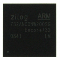
... Z32AN Series Data Sheet Chapter 22: Packaging 22.1 Soldering Information All Zilog products designated with as “Green” are RoHS compliant. 22.2 Top Mark The Top Mark contains 4 lines, as follows: Line 1: Zilog Logo and ARM Logo. Line 2: Denotes the SOC part number. Example: Z32AN12NW200XG ...
Page 196
... Chapter 23: Ordering Information The table below lists the available packages for Z32AN Series ARM SOC and provides a brief description of each product. Part Number Z32AN00NW200SG Z32AN01NW200SG Z32AN10NW200SG Please contact your local Zilog represented by this document is newly introduced and Zilog has not completed the full characterization of the product ...