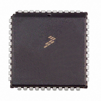
MC68HC705C9ACFN Freescale Semiconductor, MC68HC705C9ACFN Datasheet - Page 47

MC68HC705C9ACFN
Manufacturer Part Number
MC68HC705C9ACFN
Description
IC MCU 2.1MHZ 16K OTP 44-PLCC
Manufacturer
Freescale Semiconductor
Series
HC05r
Datasheet
1.MC705C9ACPE.pdf
(118 pages)
Specifications of MC68HC705C9ACFN
Core Processor
HC05
Core Size
8-Bit
Speed
2.1MHz
Connectivity
SCI, SPI
Peripherals
POR, WDT
Number Of I /o
24
Program Memory Size
16KB (16K x 8)
Program Memory Type
OTP
Ram Size
352 x 8
Voltage - Supply (vcc/vdd)
3 V ~ 5.5 V
Oscillator Type
Internal
Operating Temperature
-40°C ~ 85°C
Package / Case
44-PLCC
Lead Free Status / RoHS Status
Contains lead / RoHS non-compliant
Eeprom Size
-
Data Converters
-
Available stocks
Company
Part Number
Manufacturer
Quantity
Price
Company:
Part Number:
MC68HC705C9ACFN
Manufacturer:
Freescale Semiconductor
Quantity:
10 000
Company:
Part Number:
MC68HC705C9ACFNE
Manufacturer:
RFMD
Quantity:
8 729
Company:
Part Number:
MC68HC705C9ACFNE
Manufacturer:
Freescale Semiconductor
Quantity:
10 000
Chapter 7
Input/Output (I/O) Ports
7.1 Introduction
This section briefly describes the 31 input/output (I/O) lines arranged as one 7-bit and three 8-bit ports.
All of these port pins are programmable as either inputs or outputs under software control of the data
direction registers.
7.2 Port A
Port A is an 8-bit bidirectional port which does not share any of its pins with other subsystems. The port
A data register is at $0000 and the data direction register (DDR) is at $0004. The contents of the port A
data register are indeterminate at initial powerup and must be initialized by user software. Reset does not
affect the data registers, but clears the data direction registers, thereby returning the ports to inputs.
Writing a 1 to a DDR bit sets the corresponding port bit to output mode. A block diagram of the port logic
is shown in
Freescale Semiconductor
Figure
To avoid a glitch on the output pins, write data to the I/O port data register
before writing a one to the corresponding data direction register.
CONNECTIONS
INTERNAL
HC05
7-1.
MC68HC05C9A Advance Information Data Sheet, Rev. 4.1
LATCHED OUTPUT
DATA DIRECTION
REGISTER BIT
Figure 7-1. Port A I/O Circuit
DATA BIT
NOTE
INPUT
REG
BIT
INPUT
I/O
OUTPUT
PIN
I/O
47


