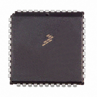
MC68HC705C9ACFN Freescale Semiconductor, MC68HC705C9ACFN Datasheet - Page 62

MC68HC705C9ACFN
Manufacturer Part Number
MC68HC705C9ACFN
Description
IC MCU 2.1MHZ 16K OTP 44-PLCC
Manufacturer
Freescale Semiconductor
Series
HC05r
Datasheet
1.MC705C9ACPE.pdf
(118 pages)
Specifications of MC68HC705C9ACFN
Core Processor
HC05
Core Size
8-Bit
Speed
2.1MHz
Connectivity
SCI, SPI
Peripherals
POR, WDT
Number Of I /o
24
Program Memory Size
16KB (16K x 8)
Program Memory Type
OTP
Ram Size
352 x 8
Voltage - Supply (vcc/vdd)
3 V ~ 5.5 V
Oscillator Type
Internal
Operating Temperature
-40°C ~ 85°C
Package / Case
44-PLCC
Lead Free Status / RoHS Status
Contains lead / RoHS non-compliant
Eeprom Size
-
Data Converters
-
Available stocks
Company
Part Number
Manufacturer
Quantity
Price
Company:
Part Number:
MC68HC705C9ACFN
Manufacturer:
Freescale Semiconductor
Quantity:
10 000
Company:
Part Number:
MC68HC705C9ACFNE
Manufacturer:
RFMD
Quantity:
8 729
Company:
Part Number:
MC68HC705C9ACFNE
Manufacturer:
Freescale Semiconductor
Quantity:
10 000
Serial Communications Interface (SCI)
9.6 Data Format
Receive data or transmit data is the serial data that is transferred to the internal data bus from the receive
data input pin (RDI) or from the internal bus to the transmit data output pin (TDO). The non-return-to-zero
(NRZ) data format shown in
9.7 Receiver Wakeup Operation
The receiver logic hardware also supports a receiver wakeup function which is intended for systems
having more than one receiver. With this function a transmitting device directs messages to an individual
receiver or group of receivers by passing addressing information as the initial byte(s) of each message.
The wakeup function allows receivers not addressed to remain in a dormant state for the remainder of the
unwanted message. This eliminates any further software overhead to service the remaining characters of
the unwanted message and thus improves system performance.
The receiver is placed in wakeup mode by setting the receiver wakeup bit (RWU) in the SCCR2 register.
While RWU is set, all of the receiver-related status flags (RDRF, IDLE, OR, NF, and FE) are inhibited
(cannot become set).
Normally, RWU is set by software and is cleared automatically in hardware by one of these methods: idle
line wakeup or address mark wakeup.
9.8 Idle Line Wakeup
In idle line wakeup mode, a dormant receiver wakes up as soon as the RDI line becomes idle. Idle is
defined as a continuous logic high level on the RDI line for 10 (or 11) full bit times. Systems using this
type of wakeup must provide at least one character time of idle between messages to wake up sleeping
receivers, but must not allow any idle time between characters within a message.
62
•
•
•
•
•
The idle line is brought to a logic 1 state prior to transmission/reception of a character.
A start bit (logic 0) is used to indicate the start of a frame.
The data is transmitted and received least significant bit first.
A stop bit (logic 1) is used to indicate the end of a frame. A frame consists of a start bit, a character
of eight or nine data bits, and a stop bit.
A break is defined as the transmission or reception of a low (logic 0) for at least one complete frame
time.
The idle line detect function is inhibited while the RWU bit is set. Although
RWU may be cleared by a software write to SCCR2, it would be unusual to
do so.
IDLE LINE
MC68HC05C9A Advance Information Data Sheet, Rev. 4.1
Figure 9-3
Figure 9-3. Data Format
is used and must meet the following criteria:
START
0
1
NOTE
2
3
4
CONTROL BIT M SELECTS
5
8- OR 9-BIT DATA
6
7
8
STOP START
0
Freescale Semiconductor


