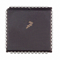
MC68HC705C9ACFN Freescale Semiconductor, MC68HC705C9ACFN Datasheet - Page 73

MC68HC705C9ACFN
Manufacturer Part Number
MC68HC705C9ACFN
Description
IC MCU 2.1MHZ 16K OTP 44-PLCC
Manufacturer
Freescale Semiconductor
Series
HC05r
Datasheet
1.MC705C9ACPE.pdf
(118 pages)
Specifications of MC68HC705C9ACFN
Core Processor
HC05
Core Size
8-Bit
Speed
2.1MHz
Connectivity
SCI, SPI
Peripherals
POR, WDT
Number Of I /o
24
Program Memory Size
16KB (16K x 8)
Program Memory Type
OTP
Ram Size
352 x 8
Voltage - Supply (vcc/vdd)
3 V ~ 5.5 V
Oscillator Type
Internal
Operating Temperature
-40°C ~ 85°C
Package / Case
44-PLCC
Lead Free Status / RoHS Status
Contains lead / RoHS non-compliant
Eeprom Size
-
Data Converters
-
Available stocks
Company
Part Number
Manufacturer
Quantity
Price
Company:
Part Number:
MC68HC705C9ACFN
Manufacturer:
Freescale Semiconductor
Quantity:
10 000
Company:
Part Number:
MC68HC705C9ACFNE
Manufacturer:
RFMD
Quantity:
8 729
Company:
Part Number:
MC68HC705C9ACFNE
Manufacturer:
Freescale Semiconductor
Quantity:
10 000
the SPSR. In master mode the SS pin can be selected to be a general-purpose output (when configured
as an MC68HC05C9A) by writing a 1 in bit 5 of the port D data direction register, thus disabling the mode
fault circuit.
When CPHA = 0, the shift clock is the OR of SS with SCK. In this clock phase mode, SS must go high
between successive characters in an SPI message. When CPHA = 1, SS may be left low for several SPI
characters. In cases where there is only one SPI slave MCU, its SS line could be tied to V
CPHA = 1 clock modes are used.
10.4 Functional Description
Figure 10-2
transmits data to a slave via the MOSI line, the slave device responds by sending data to the master
device via the master’s MISO line. This implies full duplex transmission with both data out and data in
synchronized with the same clock signal. Thus, the byte transmitted is replaced by the byte received and
eliminates the need for separate transmit-empty and receive-full status bits. A single status bit (SPIF) is
used to signify that the I/O operation has been completed.
Freescale Semiconductor
INTERNAL DATA BUS
÷ 2
shows a block diagram of the serial peripheral interface circuitry. When a master device
SPR1
INTERNAL
(XTAL ÷2)
÷ 4
DIVIDER
SELECT
CLOCK
SPI CONTROL REGISTER (SPCR)
÷ 16
SPR0
SPI STATUS REGISTER (SPSR)
Figure 10-2. Serial Peripheral Interface Block Diagram
SPI DATA REGISTER (SPDR)
÷ 32
MC68HC05C9A Advance Information Data Sheet, Rev. 4.1
SPI CLOCK (MASTER)
BIT 7
SPIE
SPIF
MSTR
7
SPIE
SPE
WCOL
BIT 6
SPE
MSTR
6
SPI SHIFT REGISTER
7 6 5 4 3 2 1 0
DWOM
CONTROL
BIT 5
CLOCK
LOGIC
CPHA
5
0
SPI
SPDR ($000C)
MSTR
MODF
BIT 4
CPOL
4
CPOL
BIT 3
3
0
(SLAVE)
WCOL
MODF
CLOCK
SPIF
CPHA
SPI
BIT 2
2
0
SPR1
SPI
CLOCK
(MASTER)
SPI INTERRUPT REQUEST
BIT 1
1
0
S
M
M
S
MISO
MOSI
PD2/
PD3/
SPR2
BIT 0
Functional Description
0
0
PD5/
$000A
$000B
$000C
PD4/
SCK
SS
SS
as long as
73


