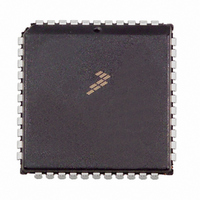
MC68HC705C9ACFN Freescale Semiconductor, MC68HC705C9ACFN Datasheet - Page 95

MC68HC705C9ACFN
Manufacturer Part Number
MC68HC705C9ACFN
Description
IC MCU 2.1MHZ 16K OTP 44-PLCC
Manufacturer
Freescale Semiconductor
Series
HC05r
Datasheet
1.MC705C9ACPE.pdf
(118 pages)
Specifications of MC68HC705C9ACFN
Core Processor
HC05
Core Size
8-Bit
Speed
2.1MHz
Connectivity
SCI, SPI
Peripherals
POR, WDT
Number Of I /o
24
Program Memory Size
16KB (16K x 8)
Program Memory Type
OTP
Ram Size
352 x 8
Voltage - Supply (vcc/vdd)
3 V ~ 5.5 V
Oscillator Type
Internal
Operating Temperature
-40°C ~ 85°C
Package / Case
44-PLCC
Lead Free Status / RoHS Status
Contains lead / RoHS non-compliant
Eeprom Size
-
Data Converters
-
Available stocks
Company
Part Number
Manufacturer
Quantity
Price
Company:
Part Number:
MC68HC705C9ACFN
Manufacturer:
Freescale Semiconductor
Quantity:
10 000
Company:
Part Number:
MC68HC705C9ACFNE
Manufacturer:
RFMD
Quantity:
8 729
Company:
Part Number:
MC68HC705C9ACFNE
Manufacturer:
Freescale Semiconductor
Quantity:
10 000
12.5 5.0-Vdc Electrical Characteristics
Freescale Semiconductor
Output voltage
Output high voltage
Output low voltage
Input high voltage
Input low voltage
Supply current (4.5–5.5 Vdc @ f
I/O ports hi-Z leakage current
Input current
Input pullup current
Capacitance
Programming voltage (25°C)
Programming current (25°C)
1. V
2. Typical values reflect measurements taken on average processed devices at the midpoint of voltage range, 25 °C only.
3. Run (operating) I
4. Wait I
5. Stop I
6. Input pullup current measured with V
I
I
(I
(I
(I
(I
(I
PA7–PA0, PB7–PB0, PC7–PC0, PD7,
PD5–PD0, TCAP, IRQ, RESET, OSC1
PA7–PA0, PB7–PB0, PC7–PC0, PD7,
PD5–PD0, TCAP, IRQ, RESET, OSC1
Run
Wait
Stop
PA7–PA0, PB7–PB0 (without pullup)
PC7–PC0, PD7, PD5–PD0
RESET, IRQ, OSC1, TCAP, PD7, PD5–PD0
PB7–PB0 (with pullup)
Ports (as input or output)
RESET, IRQ, OSC1, TCAP, PD7, PD5, PD0
L
L
other inputs V
V
by the OSC2 capacitance.
V
L
L
L
L
L
oad
oad
25°C
–40 to 85 °C
oad
oad
oad
oad
oad
DD
IL
IH
TCMP, PD7, PD0
PD7, PD5–PD0, TCMP
(3)
(4)
= 0.2 V, V
(5)
= V
= 10.0 µA
= –10.0 µA
= 5.0 Vdc ± 10%, V
= –0.8 mA) PA7–PA0, PB7–PB0, PC6–PC0,
= –1.6 mA) PD5–PD1
= –5.0 mA) PC7
= 1.6 mA) PA7–PA0, PB7–PB0, PC6–PC0,
= 10 mA) PC7
DD
DD
DD
measured using external square wave clock source; all I/O pins configured as inputs, port B = V
measured with OSC1 = 0.2 V; all I/O pins configured as inputs, port B = V
–0.2 V.
IH
IL
= V
= 0.2 V, V
(6)
DD
DD
measured using external square wave clock source; all I/O pins configured as inputs, port B = V
Characteristic
–0.2 V; no DC loads; less than 50 pF on all outputs; C
SS
IH
= 0 Vdc, T
= V
MC68HC05C9A Advance Information Data Sheet, Rev. 4.1
OP
DD
= 2.1 MHz)
–0.2 V; no DC loads; less than 50 pF on all outputs; C
(1)
A
IL
= –40 to +85 °C, unless otherwise noted
= 0.2 V.
Symbol
C
V
V
V
V
V
V
I
I
C
I
V
DD
OZ
I
I
PP
Out
OH
OH
OL
OL
In
In
PP
IH
IL
In
L
= 20 pF on OSC2. Wait I
0.7 × V
V
V
V
V
DD
DD
DD
DD
15.0
Min
V
—
—
—
—
—
—
—
—
—
—
—
—
5
–0.1
–0.8
–0.8
–0.8
SS
DD
, all other inputs V
DD
5.0-Vdc Electrical Characteristics
L
= 20 pF on OSC2
Typ
16.0
3.5
1.0
1.0
7.0
—
—
—
—
—
—
—
—
—
—
—
—
—
—
—
(2)
DD
0.2 × V
IL
is affected linearly
DD
= 0.2 V,
Max
5.25
3.25
20.0
50.0
17.0
200
V
, all other inputs
0.1
0.4
0.4
—
—
—
—
10
60
12
1
8
DD
DD
DD
Unit
mA
mA
mA
µA
µA
µA
µA
µA
pF
, all
V
V
V
V
V
V
95


