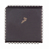
MC68HC711D3CFN2 Freescale Semiconductor, MC68HC711D3CFN2 Datasheet - Page 63

MC68HC711D3CFN2
Manufacturer Part Number
MC68HC711D3CFN2
Description
IC MCU 2MHZ 4K OTP 44-PLCC
Manufacturer
Freescale Semiconductor
Series
HC11r
Specifications of MC68HC711D3CFN2
Core Processor
HC11
Core Size
8-Bit
Speed
2MHz
Connectivity
SCI, SPI
Peripherals
POR, WDT
Number Of I /o
26
Program Memory Size
4KB (4K x 8)
Program Memory Type
OTP
Ram Size
192 x 8
Voltage - Supply (vcc/vdd)
4.5 V ~ 5.5 V
Oscillator Type
Internal
Operating Temperature
-40°C ~ 85°C
Package / Case
44-PLCC
Lead Free Status / RoHS Status
Contains lead / RoHS non-compliant
Eeprom Size
-
Data Converters
-
Available stocks
Company
Part Number
Manufacturer
Quantity
Price
Company:
Part Number:
MC68HC711D3CFN2
Manufacturer:
DIODES
Quantity:
12 000
Company:
Part Number:
MC68HC711D3CFN2
Manufacturer:
MOT
Quantity:
5 510
Company:
Part Number:
MC68HC711D3CFN2
Manufacturer:
Freescale Semiconductor
Quantity:
10 000
PORTA — Port A Data
PORTB — Port B Data
6.1 Port A
6.2 Port B
TECHNICAL DATA
Alt. Func:
RESET:
RESET:
RESET:
or Boot:
or Test:
And/or:
S. Chip
Expan.
The MC68HC11D3 has four 8-bit I/O ports; A, B, C, and D. In single-chip and bootstrap
modes, all ports are parallel I/O data ports. In expanded multiplexed and test modes,
ports B and C, and lines DATA6/AS and DATA7/R/W are a memory expansion bus
with port B as the high order address bus, port C as the multiplexed address and data
bus, AS as the demultiplexing signal, and R/W as the data bus direction control. Refer
to Table 6-1, which is a summary of the ports and their shared functions:
Port A bits handle the timer functions and can also be used as general-purpose I/O. In
both the normal operating modes, port A can be configured for four timer input capture
(IC) and three timer output compare (OC) functions, or four OC and three IC functions
with either a pulse accumulator input (PAI) or a fifth OC function.
*This pin is not bonded in the 40-pin version.
In single-chip mode, all port B pins are general-purpose I/O (PB[7:0]). In expanded
multiplexed mode, all port B pins act as high-order address bits (ADDR[15:8]).
Port C
Port D
Port A
Port B
Port
ADDR15
OC1
Bit 7
PA7
Bit 7
PB7
PB7
PAI
HiZ
Input Pins
ADDR14
PA6*
OC2
OC1
PB6
PB6
Freescale Semiconductor, Inc.
—
—
—
6
0
6
3
For More Information On This Product,
Reset configures pins as high-order address outputs
Output Pins
ADDR13
OC3
OC1
PA5
PB5
PB5
Go to: www.freescale.com
5
0
5
Table 6-1 I/O Ports
—
—
—
3
PARALLEL I/O
Reset configures pins as HiZ inputs
SECTION 6
PARALLEL I/O
ADDR12
PA4*
OC4
OC1
PB4
PB4
Bidirectional Pins
4
0
4
2
8
8
8
ADDR11
IC4/OC5
OC1
PA3
PB3
PB3
HiZ
3
3
Low Order Address and Data Bus
ADDR10
PA2
PB2
PB2
HiZ
IC1
—
2
2
SCI, SPI, AS, and R/
High Order Address
Shared Functions
TImer
ADDR9
PA1
PB1
PB1
HiZ
IC2
—
1
1
$0000
$0004
ADDR8
Bit 0
Bit 0
PA0
PB0
PB0
HiZ
IC3
—
6-1


