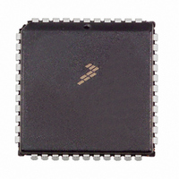
MC68HC711D3CFN2 Freescale Semiconductor, MC68HC711D3CFN2 Datasheet - Page 64

MC68HC711D3CFN2
Manufacturer Part Number
MC68HC711D3CFN2
Description
IC MCU 2MHZ 4K OTP 44-PLCC
Manufacturer
Freescale Semiconductor
Series
HC11r
Specifications of MC68HC711D3CFN2
Core Processor
HC11
Core Size
8-Bit
Speed
2MHz
Connectivity
SCI, SPI
Peripherals
POR, WDT
Number Of I /o
26
Program Memory Size
4KB (4K x 8)
Program Memory Type
OTP
Ram Size
192 x 8
Voltage - Supply (vcc/vdd)
4.5 V ~ 5.5 V
Oscillator Type
Internal
Operating Temperature
-40°C ~ 85°C
Package / Case
44-PLCC
Lead Free Status / RoHS Status
Contains lead / RoHS non-compliant
Eeprom Size
-
Data Converters
-
Available stocks
Company
Part Number
Manufacturer
Quantity
Price
Company:
Part Number:
MC68HC711D3CFN2
Manufacturer:
DIODES
Quantity:
12 000
Company:
Part Number:
MC68HC711D3CFN2
Manufacturer:
MOT
Quantity:
5 510
Company:
Part Number:
MC68HC711D3CFN2
Manufacturer:
Freescale Semiconductor
Quantity:
10 000
DDRB — Data Direction Register for Port B
PORTC — Port C Data
DDRC — Data Direction Register for Port C
DDB[7:0] — Data Direction for Port B
6.3 Port C
DDC[7:0] — Data Direction for Port C
6.4 Port D
6-2
RESET:
RESET:
RESET:
RESET:
or Boot:
or Test:
S. Chip
Expan.
Port C pins are general-purpose I/O (PC[7:0]) in single-chip mode. In expanded mul-
tiplexed mode, port C pins are configured as multiplexed address/data pins. During the
data cycle, bits [7:0] (PC[7:0]) are bidirectional data pins controlled by the R/W signal.
The eight port D bits (PD[7:0]) can be used for general-purpose I/O, for the SCI and
SPI subsystems, or for bus data direction control. Port D can be read at any time. In-
puts return the sensed levels at the pin; outputs return the input level of the port D pin
drivers. If port D is written, the data is stored in an internal latch, and can be driven only
if port D is configured for general-purpose output. This port shares functions with the
on-chip SCI and SPI subsystems, while bits 6 and 7 control the direction of data flow
on the bus in expanded and special test modes.
0 = Corresponding port B pin configured for input only
1 = Corresponding port B pin configured as output
0 = Input
1 = Output
ADDR7/
DATA7
DDC7
DDB7
Bit 7
Bit 7
PC7
PC7
Bit 7
0
0
ADDR6/
DATA6
DDC6
DDB6
PC6
PC6
Freescale Semiconductor, Inc.
6
0
6
6
0
Reset configures pins as multiplexed, low-order address/data I/O
For More Information On This Product,
ADDR5/
DATA5
DDC5
DDB5
PC5
PC5
Go to: www.freescale.com
5
0
5
5
0
Reset configures pins as HiZ inputs
PARALLEL I/O
ADDR4/
DATA4
DDC4
DDC4
PC4
PC4
4
0
4
4
0
ADDR3/
DATA3
DDC3
DDB3
PC3
PC3
3
0
3
3
0
ADDR2/
DATA2
DDC2
DDB2
PC2
PC2
2
0
2
2
0
ADDR1/
DATA1
DDC1
DDB1
PC1
PC1
TECHNICAL DATA
1
0
1
1
0
$0006
$0003
ADDR0/
$0007
DATA0
DDC0
DDB0
Bit 0
Bit 0
Bit 0
PC0
PC0
0
0


