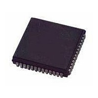
MC68HC11E1CFN3 Freescale Semiconductor, MC68HC11E1CFN3 Datasheet - Page 135

MC68HC11E1CFN3
Manufacturer Part Number
MC68HC11E1CFN3
Description
IC MCU 3MHZ 512 EEPROM 52-PLCC
Manufacturer
Freescale Semiconductor
Series
HC11r
Datasheet
1.MC68HC11E1CFN3.pdf
(268 pages)
Specifications of MC68HC11E1CFN3
Core Processor
HC11
Core Size
8-Bit
Speed
3MHz
Connectivity
SCI, SPI
Peripherals
POR, WDT
Number Of I /o
38
Program Memory Type
ROMless
Eeprom Size
512 x 8
Ram Size
512 x 8
Voltage - Supply (vcc/vdd)
4.5 V ~ 5.5 V
Data Converters
A/D 8x8b
Oscillator Type
Internal
Operating Temperature
-40°C ~ 85°C
Package / Case
52-PLCC
Data Bus Width
8 bit
Data Ram Size
512 B
Interface Type
SCI, SPI
Maximum Clock Frequency
3 MHz
Number Of Programmable I/os
22
Number Of Timers
16 bit
Maximum Operating Temperature
+ 85 C
Mounting Style
SMD/SMT
Minimum Operating Temperature
- 40 C
On-chip Adc
8 bit
Lead Free Status / RoHS Status
Contains lead / RoHS non-compliant
Program Memory Size
-
Lead Free Status / Rohs Status
Details
Available stocks
Company
Part Number
Manufacturer
Quantity
Price
Company:
Part Number:
MC68HC11E1CFN3
Manufacturer:
MOT
Quantity:
2 600
Company:
Part Number:
MC68HC11E1CFN3
Manufacturer:
MOTOROLA
Quantity:
2 337
Company:
Part Number:
MC68HC11E1CFN3
Manufacturer:
Freescale Semiconductor
Quantity:
10 000
Part Number:
MC68HC11E1CFN3
Manufacturer:
MOTOROLA/摩托罗拉
Quantity:
20 000
- Current page: 135 of 268
- Download datasheet (4Mb)
8.4 Clock Phase and Polarity Controls
8.5 SPI Signals
M68HC11E Family — Rev. 5
MOTOROLA
1. SS ASSERTED
2. MASTER WRITES TO SPDR
3. FIRST SCK EDGE
4. SPIF SET
5. SS NEGATED
(CPHA = 0)
(CPHA = 1)
SAMPLE INPUT
SAMPLE INPUT
SCK (CPOL = 0)
SCK (CPOL = 1)
SS (TO SLAVE)
SCK CYCLE #
DATA OUT
DATA OUT
Software can select one of four combinations of serial clock phase and polarity
using two bits in the SPI control register (SPCR). The clock polarity is specified by
the CPOL control bit, which selects an active high or active low clock, and has no
significant effect on the transfer format. The clock phase (CPHA) control bit selects
one of two different transfer formats. The clock phase and polarity should be
identical for the master SPI device and the communicating slave device. In some
cases, the phase and polarity are changed between transfers to allow a master
device to communicate with peripheral slaves having different requirements.
When CPHA equals 0, the SS line must be negated and reasserted between each
successive serial byte. Also, if the slave writes data to the SPI data register (SPDR)
while SS is low, a write collision error results.
When CPHA equals 1, the SS line can remain low between successive transfers.
This subsection contains descriptions of the four SPI signals:
1
•
•
•
•
2
MSB
3
Master in/slave out (MISO)
Master out/slave in (MOSI)
Serial clock (SCK)
Slave select (SS)
Freescale Semiconductor, Inc.
For More Information On This Product,
MSB
1
Figure 8-2. SPI Transfer Format
6
Serial Peripheral Interface (SPI)
Go to: www.freescale.com
2
6
SLAVE CPHA = 1 TRANSFER IN PROGRESS
SLAVE CPHA = 0 TRANSFER IN PROGRESS
5
MASTER TRANSFER IN PROGRESS
3
5
4
4
4
3
5
3
2
6
2
Clock Phase and Polarity Controls
1
Serial Peripheral Interface (SPI)
7
1
LSB
8
LSB
4
5
Data Sheet
135
Related parts for MC68HC11E1CFN3
Image
Part Number
Description
Manufacturer
Datasheet
Request
R

Part Number:
Description:
MC68HC11 EEPROM Programming from a Personal Computer
Manufacturer:
Motorola / Freescale Semiconductor
Part Number:
Description:
Manufacturer:
Freescale Semiconductor, Inc
Datasheet:
Part Number:
Description:
Manufacturer:
Freescale Semiconductor, Inc
Datasheet:
Part Number:
Description:
Manufacturer:
Freescale Semiconductor, Inc
Datasheet:
Part Number:
Description:
Manufacturer:
Freescale Semiconductor, Inc
Datasheet:
Part Number:
Description:
Manufacturer:
Freescale Semiconductor, Inc
Datasheet:
Part Number:
Description:
Manufacturer:
Freescale Semiconductor, Inc
Datasheet:
Part Number:
Description:
Manufacturer:
Freescale Semiconductor, Inc
Datasheet:
Part Number:
Description:
Manufacturer:
Freescale Semiconductor, Inc
Datasheet:
Part Number:
Description:
Manufacturer:
Freescale Semiconductor, Inc
Datasheet:
Part Number:
Description:
Manufacturer:
Freescale Semiconductor, Inc
Datasheet:
Part Number:
Description:
Manufacturer:
Freescale Semiconductor, Inc
Datasheet:
Part Number:
Description:
Manufacturer:
Freescale Semiconductor, Inc
Datasheet:
Part Number:
Description:
Manufacturer:
Freescale Semiconductor, Inc
Datasheet:
Part Number:
Description:
Manufacturer:
Freescale Semiconductor, Inc
Datasheet:


