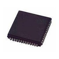
MC68HC11E1CFN3 Freescale Semiconductor, MC68HC11E1CFN3 Datasheet - Page 143

MC68HC11E1CFN3
Manufacturer Part Number
MC68HC11E1CFN3
Description
IC MCU 3MHZ 512 EEPROM 52-PLCC
Manufacturer
Freescale Semiconductor
Series
HC11r
Datasheet
1.MC68HC11E1CFN3.pdf
(268 pages)
Specifications of MC68HC11E1CFN3
Core Processor
HC11
Core Size
8-Bit
Speed
3MHz
Connectivity
SCI, SPI
Peripherals
POR, WDT
Number Of I /o
38
Program Memory Type
ROMless
Eeprom Size
512 x 8
Ram Size
512 x 8
Voltage - Supply (vcc/vdd)
4.5 V ~ 5.5 V
Data Converters
A/D 8x8b
Oscillator Type
Internal
Operating Temperature
-40°C ~ 85°C
Package / Case
52-PLCC
Data Bus Width
8 bit
Data Ram Size
512 B
Interface Type
SCI, SPI
Maximum Clock Frequency
3 MHz
Number Of Programmable I/os
22
Number Of Timers
16 bit
Maximum Operating Temperature
+ 85 C
Mounting Style
SMD/SMT
Minimum Operating Temperature
- 40 C
On-chip Adc
8 bit
Lead Free Status / RoHS Status
Contains lead / RoHS non-compliant
Program Memory Size
-
Lead Free Status / Rohs Status
Details
Available stocks
Company
Part Number
Manufacturer
Quantity
Price
Company:
Part Number:
MC68HC11E1CFN3
Manufacturer:
MOT
Quantity:
2 600
Company:
Part Number:
MC68HC11E1CFN3
Manufacturer:
MOTOROLA
Quantity:
2 337
Company:
Part Number:
MC68HC11E1CFN3
Manufacturer:
Freescale Semiconductor
Quantity:
10 000
Part Number:
MC68HC11E1CFN3
Manufacturer:
MOTOROLA/摩托罗拉
Quantity:
20 000
- Current page: 143 of 268
- Download datasheet (4Mb)
9.2 Timer Structure
M68HC11E Family — Rev. 5
MOTOROLA
The COP watchdog clock input (E ÷ 2
chain. The COP automatically times out unless it is serviced within a specific time
by a program reset sequence. If the COP is allowed to time out, a reset is
generated, which drives the RESET pin low to reset the MCU and the external
system. Refer to
Figure 9-2
control block includes logic for timer functions and for general-purpose I/O. For pins
PA3, PA2, PA1, and PA0, this block contains both the edge-detection logic and the
control logic that enables the selection of which edge triggers an input capture. The
digital level on PA[3:0] can be read at any time (read PORTA register), even if the
pin is being used for the input capture function. Pins PA[6:3] are used for either
general-purpose I/O, or as output compare pins. When one of these pins is being
used for an output compare function, it cannot be written directly as if it were a
general-purpose output. Each of the output compare functions (OC[5:2]) is related
to one of the port A output pins. Output compare one (OC1) has extra control logic,
allowing it optional control of any combination of the PA[7:3] pins. The PA7 pin can
be used as a general-purpose I/O pin, as an input to the pulse accumulator, or as
an OC1 output pin.
Control Bits
overflow —
overflow —
overflow —
overflow —
1 count —
1 count —
1 count —
1 count —
PR1, PR0
Freescale Semiconductor, Inc.
0 0
0 1
1 0
1 1
For More Information On This Product,
shows the capture/compare system block diagram. The port A pin
Table 9-1
Go to: www.freescale.com
65.536 ms
262.14 ms
524.29 ms
4.0 MHz
1.0 MHz
1000 ns
1000 ns
16.0 µs
1.049 s
4.0 µs
8.0 µs
Timing System
Table 9-1. Timer Summary
for crystal-related frequencies and periods.
32.768 ms
131.07 ms
262.14 ms
524.29 ms
8.0 MHz
2.0 MHz
15
500 ns
500 ns
Main Timer Count Rates
2.0 µs
4.0 µs
8.0 µs
) is tapped off of the free-running counter
XTAL Frequencies
21.845 ms
87.381 ms
174.76 ms
349.52 ms
12.0 MHz
1.333 µs
2.667 µs
5.333 µs
3.0 MHz
333 ns
333 ns
Timer Structure
Timing System
Other Rates
(E/2
(E/2
(E/2
(E/2
(E/16)
(1/E)
(E/1)
(E/4)
(E/8)
(E)
Data Sheet
16
18
19
20
)
)
)
)
143
Related parts for MC68HC11E1CFN3
Image
Part Number
Description
Manufacturer
Datasheet
Request
R

Part Number:
Description:
MC68HC11 EEPROM Programming from a Personal Computer
Manufacturer:
Motorola / Freescale Semiconductor
Part Number:
Description:
Manufacturer:
Freescale Semiconductor, Inc
Datasheet:
Part Number:
Description:
Manufacturer:
Freescale Semiconductor, Inc
Datasheet:
Part Number:
Description:
Manufacturer:
Freescale Semiconductor, Inc
Datasheet:
Part Number:
Description:
Manufacturer:
Freescale Semiconductor, Inc
Datasheet:
Part Number:
Description:
Manufacturer:
Freescale Semiconductor, Inc
Datasheet:
Part Number:
Description:
Manufacturer:
Freescale Semiconductor, Inc
Datasheet:
Part Number:
Description:
Manufacturer:
Freescale Semiconductor, Inc
Datasheet:
Part Number:
Description:
Manufacturer:
Freescale Semiconductor, Inc
Datasheet:
Part Number:
Description:
Manufacturer:
Freescale Semiconductor, Inc
Datasheet:
Part Number:
Description:
Manufacturer:
Freescale Semiconductor, Inc
Datasheet:
Part Number:
Description:
Manufacturer:
Freescale Semiconductor, Inc
Datasheet:
Part Number:
Description:
Manufacturer:
Freescale Semiconductor, Inc
Datasheet:
Part Number:
Description:
Manufacturer:
Freescale Semiconductor, Inc
Datasheet:
Part Number:
Description:
Manufacturer:
Freescale Semiconductor, Inc
Datasheet:


