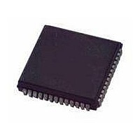
MC68HC11E1CFN3 Freescale Semiconductor, MC68HC11E1CFN3 Datasheet - Page 184

MC68HC11E1CFN3
Manufacturer Part Number
MC68HC11E1CFN3
Description
IC MCU 3MHZ 512 EEPROM 52-PLCC
Manufacturer
Freescale Semiconductor
Series
HC11r
Datasheet
1.MC68HC11E1CFN3.pdf
(268 pages)
Specifications of MC68HC11E1CFN3
Core Processor
HC11
Core Size
8-Bit
Speed
3MHz
Connectivity
SCI, SPI
Peripherals
POR, WDT
Number Of I /o
38
Program Memory Type
ROMless
Eeprom Size
512 x 8
Ram Size
512 x 8
Voltage - Supply (vcc/vdd)
4.5 V ~ 5.5 V
Data Converters
A/D 8x8b
Oscillator Type
Internal
Operating Temperature
-40°C ~ 85°C
Package / Case
52-PLCC
Data Bus Width
8 bit
Data Ram Size
512 B
Interface Type
SCI, SPI
Maximum Clock Frequency
3 MHz
Number Of Programmable I/os
22
Number Of Timers
16 bit
Maximum Operating Temperature
+ 85 C
Mounting Style
SMD/SMT
Minimum Operating Temperature
- 40 C
On-chip Adc
8 bit
Lead Free Status / RoHS Status
Contains lead / RoHS non-compliant
Program Memory Size
-
Lead Free Status / Rohs Status
Details
Available stocks
Company
Part Number
Manufacturer
Quantity
Price
Company:
Part Number:
MC68HC11E1CFN3
Manufacturer:
MOT
Quantity:
2 600
Company:
Part Number:
MC68HC11E1CFN3
Manufacturer:
MOTOROLA
Quantity:
2 337
Company:
Part Number:
MC68HC11E1CFN3
Manufacturer:
Freescale Semiconductor
Quantity:
10 000
Part Number:
MC68HC11E1CFN3
Manufacturer:
MOTOROLA/摩托罗拉
Quantity:
20 000
Electrical Characteristics
10.15 Expansion Bus Timing Characteristics
Data Sheet
184
Num
1. V
2. Formula only for dc to 2 MHz
3. Input clocks with duty cycles other than 50% affect bus performance. Timing parameters affected by input clock duty cycle
Where:
4a
4b
12
17
18
19
21
22
24
25
26
27
28
29
35
36
1
2
3
9
otherwise noted
are identified by (a) and (b). To recalculate the approximate bus timing values, substitute the following expressions in place
of 1/8 t
(a) (1–dc) × 1/4 t
(b) dc × 1/4 t
dc is the decimal value of duty cycle percentage (high time)
DD
Frequency of operation (E-clock frequency)
Cycle time
Pulse width, E low
Pulse width, E high
E and AS rise time
E and AS fall time
Address hold time
Non-multiplexed address valid time to E rise
Read data setup time
Read data hold time, max = t
Write data delay time, t
Write data hold time, t
Multiplexed address valid time to E rise
Multiplexed address valid time to AS fall
Multiplexed address hold time
Delay time, E to AS rise, t
Pulse width, AS high, PW
Delay time, AS to E rise, t
MPU address access time
MPU access time, t
Multiplexed address delay (Previous cycle MPU read)
= 5.0 Vdc ±10%, V
t
t
t
t
t
t
AV
AVM
ASL
AHL
ACCA
MAD
CYC
= PW
= PW
= 1/8 t
= PW
= t
in the above formulas, where applicable:
= t
CYC
ASD
CYC
EL
ASH
EL
CYC
CYC
–(t
+ 30 ns
–(PW
–(t
ASD
–70 ns
–29.5 ns
ASD
(2) (3)a
(2)
(2)
ACCE
SS
EL
Characteristic
, PW
+ 80 ns)
, PW
(2) (3)a
DHW
+ 90 ns)
–t
= 0 Vdc, T
DDW
(2)
, t
AVM
= PW
EL
(2) (3)b
ASH
ASD
ASED
AH
EH
(3)a
= 1/8 t
Freescale Semiconductor, Inc.
= 1/8 t
) –t
= 1/2 t
(2) (3)a
MAD
= 1/8 t
= 1/2 t
= 1/4 t
For More Information On This Product,
= 1/8 t
(2) (3)a
EH
= 1/8 t
DSR
CYC
A
–t
CYC
CYC
= T
–t
CYC
DSR
(1)
CYC
CYC
CYC
–29.5 ns
f
CYC
+ 65.5 ns
L
–23 ns
–29.5 ns
–28 ns
to T
Go to: www.freescale.com
–9.5 ns
–29 ns
–9.5 ns
Electrical Characteristics
H
, all timing is shown with respect to 20% V
(2) (3)a
(2)
(2) (3)a
(2) (3)a
(2) (3)b
Symbol
PW
PW
PW
t
t
t
t
t
t
t
t
t
t
t
t
ASED
ACCA
ACCE
t
DDW
DHW
CYC
DSR
DHR
AVM
MAD
t
t
AHL
ASD
ASL
AH
AV
f
t
t
o
ASH
r
f
EH
EL
281.5
271.5
115.5
115.5
744.5
145.5
1000
95.5
95.5
95.5
Min
477
472
151
221
dc
—
—
30
—
—
0
1.0 MHz
145.5
190.5
Max
442
1.0
20
20
—
—
—
—
—
—
—
—
—
—
—
—
—
—
—
DD
Min Max Min Max
500
227
222
307
33
94
30
33
84
26
33
53
96
53
83
dc
—
—
—
—
2.0 MHz
0
M68HC11E Family — Rev. 5
and 70% V
128
192
2.0
20
20
83
—
—
—
—
—
—
—
—
—
—
—
—
—
—
—
333
146
141
196
dc
—
—
26
54
30
26
54
13
31
31
63
31
51
3.0 MHz
0
DD
, unless
MOTOROLA
111
3.0
20
15
51
71
—
—
—
—
—
—
—
—
—
—
—
—
—
—
—
MHz
Unit
ns
ns
ns
ns
ns
ns
ns
ns
ns
ns
ns
ns
ns
ns
ns
ns
ns
ns
ns
ns


