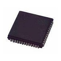
MC68HC11E1CFN3 Freescale Semiconductor, MC68HC11E1CFN3 Datasheet - Page 222

MC68HC11E1CFN3
Manufacturer Part Number
MC68HC11E1CFN3
Description
IC MCU 3MHZ 512 EEPROM 52-PLCC
Manufacturer
Freescale Semiconductor
Series
HC11r
Datasheet
1.MC68HC11E1CFN3.pdf
(268 pages)
Specifications of MC68HC11E1CFN3
Core Processor
HC11
Core Size
8-Bit
Speed
3MHz
Connectivity
SCI, SPI
Peripherals
POR, WDT
Number Of I /o
38
Program Memory Type
ROMless
Eeprom Size
512 x 8
Ram Size
512 x 8
Voltage - Supply (vcc/vdd)
4.5 V ~ 5.5 V
Data Converters
A/D 8x8b
Oscillator Type
Internal
Operating Temperature
-40°C ~ 85°C
Package / Case
52-PLCC
Data Bus Width
8 bit
Data Ram Size
512 B
Interface Type
SCI, SPI
Maximum Clock Frequency
3 MHz
Number Of Programmable I/os
22
Number Of Timers
16 bit
Maximum Operating Temperature
+ 85 C
Mounting Style
SMD/SMT
Minimum Operating Temperature
- 40 C
On-chip Adc
8 bit
Lead Free Status / RoHS Status
Contains lead / RoHS non-compliant
Program Memory Size
-
Lead Free Status / Rohs Status
Details
Available stocks
Company
Part Number
Manufacturer
Quantity
Price
Company:
Part Number:
MC68HC11E1CFN3
Manufacturer:
MOT
Quantity:
2 600
Company:
Part Number:
MC68HC11E1CFN3
Manufacturer:
MOTOROLA
Quantity:
2 337
Company:
Part Number:
MC68HC11E1CFN3
Manufacturer:
Freescale Semiconductor
Quantity:
10 000
Part Number:
MC68HC11E1CFN3
Manufacturer:
MOTOROLA/摩托罗拉
Quantity:
20 000
- Current page: 222 of 268
- Download datasheet (4Mb)
Freescale Semiconductor, Inc.
Application Note
To understand the detailed operation of the EPROM programming utility,
refer to
Figure 4
during the following discussion.
Figure 4
is composed
of three interrelated parts. The upper-left portion shows the flowchart of
the PROGRAM utility running in the boot ROM of the MCU. The upper-
right portion shows the flowchart for the user-supplied driver program
running in the host computer. The lower portion of
Figure 4
is a timing
sequence showing the relationship of operations between the MCU and
the host computer. Reference numbers in the flowcharts in the upper
half of
Figure 4
have matching numbers in the lower half to help the
reader relate the three parts of the figure.
The shaded area [1] refers to the software and hardware latency in the
MCU leading to the transmission of a character (in this case, the $FF).
The shaded area [2] refers to a similar latency in the host computer (in
this case, leading to the transmission of the first data character to the
MCU).
The overall operation begins when the MCU sends the first character
($FF) to the host computer, indicating that it is ready for the first data
character. The host computer sends the first data byte [3] and enters its
main loop. The second data character is sent [4], and the host then waits
[5] for the first verify byte to come back from the MCU.
After the MCU sends $FF [8], it enters the WAIT1 loop [9] and waits for
the first data character from the host. When this character is received
[10], the MCU programs it into the address pointed to by the Y index
register. When the programming time delay is over, the MCU reads the
programmed data, transmits it to the host for verification [11], and
returns to the top of the WAIT1 loop to wait for the next data character
[12]. Because the host previously sent the second data character, it is
already waiting in the SCI receiver of the MCU. Steps [13], [14], and [15]
correspond to the second pass through the WAIT1 loop.
Back in the host, the first verify character is received, and the third data
character is sent [6]. The host then waits for the second verify character
[7] to come back from the MCU. The sequence continues as long as the
host continues to send data to the MCU. Since the WAIT1 loop in the
PROGRAM utility is an indefinite loop, reset is used to end the process
in the MCU after the host has finished sending data to be programmed.
AN1060 — Rev. 1.0
222
MOTOROLA
For More Information On This Product,
Go to: www.freescale.com
Related parts for MC68HC11E1CFN3
Image
Part Number
Description
Manufacturer
Datasheet
Request
R

Part Number:
Description:
MC68HC11 EEPROM Programming from a Personal Computer
Manufacturer:
Motorola / Freescale Semiconductor
Part Number:
Description:
Manufacturer:
Freescale Semiconductor, Inc
Datasheet:
Part Number:
Description:
Manufacturer:
Freescale Semiconductor, Inc
Datasheet:
Part Number:
Description:
Manufacturer:
Freescale Semiconductor, Inc
Datasheet:
Part Number:
Description:
Manufacturer:
Freescale Semiconductor, Inc
Datasheet:
Part Number:
Description:
Manufacturer:
Freescale Semiconductor, Inc
Datasheet:
Part Number:
Description:
Manufacturer:
Freescale Semiconductor, Inc
Datasheet:
Part Number:
Description:
Manufacturer:
Freescale Semiconductor, Inc
Datasheet:
Part Number:
Description:
Manufacturer:
Freescale Semiconductor, Inc
Datasheet:
Part Number:
Description:
Manufacturer:
Freescale Semiconductor, Inc
Datasheet:
Part Number:
Description:
Manufacturer:
Freescale Semiconductor, Inc
Datasheet:
Part Number:
Description:
Manufacturer:
Freescale Semiconductor, Inc
Datasheet:
Part Number:
Description:
Manufacturer:
Freescale Semiconductor, Inc
Datasheet:
Part Number:
Description:
Manufacturer:
Freescale Semiconductor, Inc
Datasheet:
Part Number:
Description:
Manufacturer:
Freescale Semiconductor, Inc
Datasheet:


