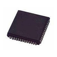
MC68HC11E1CFN3 Freescale Semiconductor, MC68HC11E1CFN3 Datasheet - Page 47

MC68HC11E1CFN3
Manufacturer Part Number
MC68HC11E1CFN3
Description
IC MCU 3MHZ 512 EEPROM 52-PLCC
Manufacturer
Freescale Semiconductor
Series
HC11r
Datasheet
1.MC68HC11E1CFN3.pdf
(268 pages)
Specifications of MC68HC11E1CFN3
Core Processor
HC11
Core Size
8-Bit
Speed
3MHz
Connectivity
SCI, SPI
Peripherals
POR, WDT
Number Of I /o
38
Program Memory Type
ROMless
Eeprom Size
512 x 8
Ram Size
512 x 8
Voltage - Supply (vcc/vdd)
4.5 V ~ 5.5 V
Data Converters
A/D 8x8b
Oscillator Type
Internal
Operating Temperature
-40°C ~ 85°C
Package / Case
52-PLCC
Data Bus Width
8 bit
Data Ram Size
512 B
Interface Type
SCI, SPI
Maximum Clock Frequency
3 MHz
Number Of Programmable I/os
22
Number Of Timers
16 bit
Maximum Operating Temperature
+ 85 C
Mounting Style
SMD/SMT
Minimum Operating Temperature
- 40 C
On-chip Adc
8 bit
Lead Free Status / RoHS Status
Contains lead / RoHS non-compliant
Program Memory Size
-
Lead Free Status / Rohs Status
Details
Available stocks
Company
Part Number
Manufacturer
Quantity
Price
Company:
Part Number:
MC68HC11E1CFN3
Manufacturer:
MOT
Quantity:
2 600
Company:
Part Number:
MC68HC11E1CFN3
Manufacturer:
MOTOROLA
Quantity:
2 337
Company:
Part Number:
MC68HC11E1CFN3
Manufacturer:
Freescale Semiconductor
Quantity:
10 000
Part Number:
MC68HC11E1CFN3
Manufacturer:
MOTOROLA/摩托罗拉
Quantity:
20 000
- Current page: 47 of 268
- Download datasheet (4Mb)
2.3.3 System Initialization
M68HC11E Family — Rev. 5
MOTOROLA
SMOD = 0
SMOD = 1
Operating
Mode
Register
Address
$x03C
$x03D
$x03C
$x03D
$x024
$x035
$x039
$x024
$x035
$x039
Timer interrupt mask 2 (TMSK2)
Block protect register (BPROT)
System configuration options (OPTION)
Highest priority I-bit interrupt
and miscellaneous (HPRIO)
RAM and I/O map register (INIT)
Timer interrupt mask 2 (TMSK2)
Block protect register (BPROT)
System configuration options (OPTION)
Highest priority I-bit interrupt and
miscellaneous (HPRIO)
RAM and I/O map register (INIT)
IRV(NE) — Internal Read Visibility (Not E) Bit
PSEL[3:0] — Priority Select Bits
Registers and bits that control initialization and the basic operation of the MCU are
protected against writes except under special circumstances.
registers that can be written only once after reset or that must be written within the
first 64 cycles after reset.
IRVNE can be written once in any mode. In expanded modes, IRVNE
determines whether IRV is on or off. In special test mode, IRVNE is reset to 1.
In all other modes, IRVNE is reset to 0. For the MC68HC811E2, this bit is IRV
and only controls the internal read visibility function.
In single-chip modes this bit determines whether the E clock drives out from the
chip. For the MC68HC811E2, this bit has no meaning or effect in single-chip and
bootstrap modes.
Refer to
Special test
Single chip
Expanded
0 = No internal read visibility on external bus
1 = Data from internal reads is driven out the external data bus.
0 = E is driven out from the chip.
1 = E pin is driven low. Refer to the following table.
Bootstrap
Freescale Semiconductor, Inc.
Table 2-2. Write Access Limited Registers
Mode
Register Name
For More Information On This Product,
Section 5. Resets and
Operating Modes and On-Chip Memory
Go to: www.freescale.com
IRVNE Out
of Reset
0
0
0
1
E Clock Out
of Reset
Bits [1:0], once only
Clear bits, once only
Bits [5:4], bits [2:0], once only
See HPRIO description
Yes, once only
See HPRIO description
On
On
On
On
Interrupts.
in First 64 Cycles
Must be Written
of Reset
IRV Out
Operating Modes and On-Chip Memory
—
—
—
—
Off
Off
Off
On
Affects Only
IRVNE
IRV
IRV
Bits [7:2]
Set bits only
Bits [7:6], bit 3
See HPRIO description
All, set or clear
All, set or clear
All, set or clear
See HPRIO description
All, set or clear
E
E
Table 2-2
Anytime
Write
Memory Map
—
IRVNE Can
Be Written
lists
Data Sheet
Once
Once
Once
Once
47
Related parts for MC68HC11E1CFN3
Image
Part Number
Description
Manufacturer
Datasheet
Request
R

Part Number:
Description:
MC68HC11 EEPROM Programming from a Personal Computer
Manufacturer:
Motorola / Freescale Semiconductor
Part Number:
Description:
Manufacturer:
Freescale Semiconductor, Inc
Datasheet:
Part Number:
Description:
Manufacturer:
Freescale Semiconductor, Inc
Datasheet:
Part Number:
Description:
Manufacturer:
Freescale Semiconductor, Inc
Datasheet:
Part Number:
Description:
Manufacturer:
Freescale Semiconductor, Inc
Datasheet:
Part Number:
Description:
Manufacturer:
Freescale Semiconductor, Inc
Datasheet:
Part Number:
Description:
Manufacturer:
Freescale Semiconductor, Inc
Datasheet:
Part Number:
Description:
Manufacturer:
Freescale Semiconductor, Inc
Datasheet:
Part Number:
Description:
Manufacturer:
Freescale Semiconductor, Inc
Datasheet:
Part Number:
Description:
Manufacturer:
Freescale Semiconductor, Inc
Datasheet:
Part Number:
Description:
Manufacturer:
Freescale Semiconductor, Inc
Datasheet:
Part Number:
Description:
Manufacturer:
Freescale Semiconductor, Inc
Datasheet:
Part Number:
Description:
Manufacturer:
Freescale Semiconductor, Inc
Datasheet:
Part Number:
Description:
Manufacturer:
Freescale Semiconductor, Inc
Datasheet:
Part Number:
Description:
Manufacturer:
Freescale Semiconductor, Inc
Datasheet:


