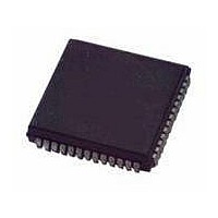
MC68HC11E1CFN3 Freescale Semiconductor, MC68HC11E1CFN3 Datasheet - Page 63

MC68HC11E1CFN3
Manufacturer Part Number
MC68HC11E1CFN3
Description
IC MCU 3MHZ 512 EEPROM 52-PLCC
Manufacturer
Freescale Semiconductor
Series
HC11r
Datasheet
1.MC68HC11E1CFN3.pdf
(268 pages)
Specifications of MC68HC11E1CFN3
Core Processor
HC11
Core Size
8-Bit
Speed
3MHz
Connectivity
SCI, SPI
Peripherals
POR, WDT
Number Of I /o
38
Program Memory Type
ROMless
Eeprom Size
512 x 8
Ram Size
512 x 8
Voltage - Supply (vcc/vdd)
4.5 V ~ 5.5 V
Data Converters
A/D 8x8b
Oscillator Type
Internal
Operating Temperature
-40°C ~ 85°C
Package / Case
52-PLCC
Data Bus Width
8 bit
Data Ram Size
512 B
Interface Type
SCI, SPI
Maximum Clock Frequency
3 MHz
Number Of Programmable I/os
22
Number Of Timers
16 bit
Maximum Operating Temperature
+ 85 C
Mounting Style
SMD/SMT
Minimum Operating Temperature
- 40 C
On-chip Adc
8 bit
Lead Free Status / RoHS Status
Contains lead / RoHS non-compliant
Program Memory Size
-
Lead Free Status / Rohs Status
Details
Available stocks
Company
Part Number
Manufacturer
Quantity
Price
Company:
Part Number:
MC68HC11E1CFN3
Manufacturer:
MOT
Quantity:
2 600
Company:
Part Number:
MC68HC11E1CFN3
Manufacturer:
MOTOROLA
Quantity:
2 337
Company:
Part Number:
MC68HC11E1CFN3
Manufacturer:
Freescale Semiconductor
Quantity:
10 000
Part Number:
MC68HC11E1CFN3
Manufacturer:
MOTOROLA/摩托罗拉
Quantity:
20 000
- Current page: 63 of 268
- Download datasheet (4Mb)
3.1 Introduction
3.2 Overview
3.2.1 Multiplexer
M68HC11E Family — Rev. 5
MOTOROLA
Data Sheet — M68HC11E Family
The analog-to-digital (A/D) system, a successive approximation converter, uses an
all-capacitive charge redistribution technique to convert analog signals to digital
values.
The A/D system is an 8-channel, 8-bit, multiplexed-input converter. The converter
does not require external sample and hold circuits because of the type of charge
redistribution technique used. A/D converter timing can be synchronized to the
system E clock or to an internal resistor capacitor (RC) oscillator.
The A/D converter system consists of four functional blocks: multiplexer, analog
converter, digital control, and result storage. Refer to
The multiplexer selects one of 16 inputs for conversion. Input selection is controlled
by the value of bits CD:CA in the ADCTL register. The eight port E pins are
fixed-direction analog inputs to the multiplexer, and additional internal analog
signal lines are routed to it.
Port E pins also can be used as digital inputs. Digital reads of port E pins are not
recommended during the sample portion of an A/D conversion cycle, when the
gate signal to the N-channel input gate is on. Because no P-channel devices are
directly connected to either input pins or reference voltage pins, voltages above
V
to maximum ratings. Refer to
input pin.
DD
do not cause a latchup problem, although current should be limited according
Freescale Semiconductor, Inc.
For More Information On This Product,
Analog-to-Digital (A/D) Converter
Go to: www.freescale.com
Section 3. Analog-to-Digital (A/D) Converter
Figure
3-2, which is a functional diagram of an
Figure
3-1.
Data Sheet
63
Related parts for MC68HC11E1CFN3
Image
Part Number
Description
Manufacturer
Datasheet
Request
R

Part Number:
Description:
MC68HC11 EEPROM Programming from a Personal Computer
Manufacturer:
Motorola / Freescale Semiconductor
Part Number:
Description:
Manufacturer:
Freescale Semiconductor, Inc
Datasheet:
Part Number:
Description:
Manufacturer:
Freescale Semiconductor, Inc
Datasheet:
Part Number:
Description:
Manufacturer:
Freescale Semiconductor, Inc
Datasheet:
Part Number:
Description:
Manufacturer:
Freescale Semiconductor, Inc
Datasheet:
Part Number:
Description:
Manufacturer:
Freescale Semiconductor, Inc
Datasheet:
Part Number:
Description:
Manufacturer:
Freescale Semiconductor, Inc
Datasheet:
Part Number:
Description:
Manufacturer:
Freescale Semiconductor, Inc
Datasheet:
Part Number:
Description:
Manufacturer:
Freescale Semiconductor, Inc
Datasheet:
Part Number:
Description:
Manufacturer:
Freescale Semiconductor, Inc
Datasheet:
Part Number:
Description:
Manufacturer:
Freescale Semiconductor, Inc
Datasheet:
Part Number:
Description:
Manufacturer:
Freescale Semiconductor, Inc
Datasheet:
Part Number:
Description:
Manufacturer:
Freescale Semiconductor, Inc
Datasheet:
Part Number:
Description:
Manufacturer:
Freescale Semiconductor, Inc
Datasheet:
Part Number:
Description:
Manufacturer:
Freescale Semiconductor, Inc
Datasheet:


