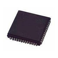
MC68HC11E1CFN3 Freescale Semiconductor, MC68HC11E1CFN3 Datasheet - Page 75

MC68HC11E1CFN3
Manufacturer Part Number
MC68HC11E1CFN3
Description
IC MCU 3MHZ 512 EEPROM 52-PLCC
Manufacturer
Freescale Semiconductor
Series
HC11r
Datasheet
1.MC68HC11E1CFN3.pdf
(268 pages)
Specifications of MC68HC11E1CFN3
Core Processor
HC11
Core Size
8-Bit
Speed
3MHz
Connectivity
SCI, SPI
Peripherals
POR, WDT
Number Of I /o
38
Program Memory Type
ROMless
Eeprom Size
512 x 8
Ram Size
512 x 8
Voltage - Supply (vcc/vdd)
4.5 V ~ 5.5 V
Data Converters
A/D 8x8b
Oscillator Type
Internal
Operating Temperature
-40°C ~ 85°C
Package / Case
52-PLCC
Data Bus Width
8 bit
Data Ram Size
512 B
Interface Type
SCI, SPI
Maximum Clock Frequency
3 MHz
Number Of Programmable I/os
22
Number Of Timers
16 bit
Maximum Operating Temperature
+ 85 C
Mounting Style
SMD/SMT
Minimum Operating Temperature
- 40 C
On-chip Adc
8 bit
Lead Free Status / RoHS Status
Contains lead / RoHS non-compliant
Program Memory Size
-
Lead Free Status / Rohs Status
Details
Available stocks
Company
Part Number
Manufacturer
Quantity
Price
Company:
Part Number:
MC68HC11E1CFN3
Manufacturer:
MOT
Quantity:
2 600
Company:
Part Number:
MC68HC11E1CFN3
Manufacturer:
MOTOROLA
Quantity:
2 337
Company:
Part Number:
MC68HC11E1CFN3
Manufacturer:
Freescale Semiconductor
Quantity:
10 000
Part Number:
MC68HC11E1CFN3
Manufacturer:
MOTOROLA/摩托罗拉
Quantity:
20 000
4.2.2 Index Register X (IX)
4.2.3 Index Register Y (IY)
4.2.4 Stack Pointer (SP)
M68HC11E Family — Rev. 5
MOTOROLA
The IX register provides a 16-bit indexing value that can be added to the 8-bit offset
provided in an instruction to create an effective address. The IX register can also
be used as a counter or as a temporary storage register.
The 16-bit IY register performs an indexed mode function similar to that of the IX
register. However, most instructions using the IY register require an extra byte of
machine code and an extra cycle of execution time because of the way the opcode
map is implemented. Refer to
The M68HC11 CPU has an automatic program stack. This stack can be located
anywhere in the address space and can be any size up to the amount of memory
available in the system. Normally, the SP is initialized by one of the first instructions
in an application program. The stack is configured as a data structure that grows
downward from high memory to low memory. Each time a new byte is pushed onto
the stack, the SP is decremented. Each time a byte is pulled from the stack, the SP
is incremented. At any given time, the SP holds the 16-bit address of the next free
location in the stack.
When a subroutine is called by a jump-to-subroutine (JSR) or branch-to-
subroutine (BSR) instruction, the address of the instruction after the JSR or BSR
is automatically pushed onto the stack, least significant byte first. When the
subroutine is finished, a return-from-subroutine (RTS) instruction is executed. The
RTS pulls the previously stacked return address from the stack and loads it into the
program counter. Execution then continues at this recovered return address.
When an interrupt is recognized, the current instruction finishes normally, the
return address (the current value in the program counter) is pushed onto the stack,
all of the CPU registers are pushed onto the stack, and execution continues at the
address specified by the vector for the interrupt.
At the end of the interrupt service routine, an return-from interrupt (RTI) instruction
is executed. The RTI instruction causes the saved registers to be pulled off the
stack in reverse order. Program execution resumes at the return address.
Certain instructions push and pull the A and B accumulators and the X and Y index
registers and are often used to preserve program context. For example, pushing
accumulator A onto the stack when entering a subroutine that uses accumulator A
and then pulling accumulator A off the stack just before leaving the subroutine
ensures that the contents of a register will be the same after returning from the
subroutine as it was before starting the subroutine.
Freescale Semiconductor, Inc.
For More Information On This Product,
Go to: www.freescale.com
Central Processor Unit (CPU)
Figure 4-2
4.4 Opcodes and Operands
is a summary of SP operations.
Central Processor Unit (CPU)
for further information.
CPU Registers
Data Sheet
75


