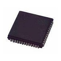
MC68HC11E1CFN3 Freescale Semiconductor, MC68HC11E1CFN3 Datasheet - Page 87

MC68HC11E1CFN3
Manufacturer Part Number
MC68HC11E1CFN3
Description
IC MCU 3MHZ 512 EEPROM 52-PLCC
Manufacturer
Freescale Semiconductor
Series
HC11r
Datasheet
1.MC68HC11E1CFN3.pdf
(268 pages)
Specifications of MC68HC11E1CFN3
Core Processor
HC11
Core Size
8-Bit
Speed
3MHz
Connectivity
SCI, SPI
Peripherals
POR, WDT
Number Of I /o
38
Program Memory Type
ROMless
Eeprom Size
512 x 8
Ram Size
512 x 8
Voltage - Supply (vcc/vdd)
4.5 V ~ 5.5 V
Data Converters
A/D 8x8b
Oscillator Type
Internal
Operating Temperature
-40°C ~ 85°C
Package / Case
52-PLCC
Data Bus Width
8 bit
Data Ram Size
512 B
Interface Type
SCI, SPI
Maximum Clock Frequency
3 MHz
Number Of Programmable I/os
22
Number Of Timers
16 bit
Maximum Operating Temperature
+ 85 C
Mounting Style
SMD/SMT
Minimum Operating Temperature
- 40 C
On-chip Adc
8 bit
Lead Free Status / RoHS Status
Contains lead / RoHS non-compliant
Program Memory Size
-
Lead Free Status / Rohs Status
Details
Available stocks
Company
Part Number
Manufacturer
Quantity
Price
Company:
Part Number:
MC68HC11E1CFN3
Manufacturer:
MOT
Quantity:
2 600
Company:
Part Number:
MC68HC11E1CFN3
Manufacturer:
MOTOROLA
Quantity:
2 337
Company:
Part Number:
MC68HC11E1CFN3
Manufacturer:
Freescale Semiconductor
Quantity:
10 000
Part Number:
MC68HC11E1CFN3
Manufacturer:
MOTOROLA/摩托罗拉
Quantity:
20 000
M68HC11E Family — Rev. 5
MOTOROLA
Cycle
*
**
Operands
dd
ff
hh
ii
jj
kk
ll
mm
rr
Operators
( )
⇐
⇑
⇓
•
+
⊕
∗
:
–
Mnemonic
TST (opr)
XGDX
XGDY
TEST
TSTA
TSTB
SWI
TAB
TAP
TBA
TPA
TSX
TSY
TXS
TYS
WAI
Infinity or until reset occurs
12 cycles are used beginning with the opcode fetch. A wait state is entered which remains in effect for an integer number of MPU E-clock
cycles (n) until an interrupt is recognized. Finally, two additional cycles are used to fetch the appropriate interrupt vector (14 + n total).
= 8-bit direct address ($0000–$00FF) (high byte assumed to be $00)
= 8-bit positive offset $00 (0) to $FF (255) (is added to index)
= High-order byte of 16-bit extended address
= One byte of immediate data
= High-order byte of 16-bit immediate data
= Low-order byte of 16-bit immediate data
= Low-order byte of 16-bit extended address
= 8-bit mask (set bits to be affected)
= Signed relative offset $80 (–128) to $7F (+127)
Contents of register shown inside parentheses
Is transferred to
Is pulled from stack
Is pushed onto stack
Boolean AND
Arithmetic addition symbol except where used as inclusive-OR symbol
in Boolean formula
Exclusive-OR
Multiply
Concatenation
Arithmetic subtraction symbol or negation symbol (two’s complement)
(offset relative to address following machine code offset byte))
Test for Zero or
Transfer A to B
Transfer B to A
Test A for Zero
Test B for Zero
Transfer Stack
Transfer Stack
TEST (Only in
Stack Pointer
Stack Pointer
Transfer A to
Register to A
Transfer X to
Transfer Y to
Test Modes)
CC Register
Transfer CC
Exchange D
Exchange D
Pointer to X
Pointer to Y
Operation
Software
or Minus
or Minus
Interrupt
Interrupt
Wait for
with X
with Y
Minus
Address Bus Counts
Stack Regs & WAIT
IX ⇒ D, D ⇒ IX
IY ⇒ D, D ⇒ IY
See Figure 3–2
Description
SP + 1 ⇒ IX
SP + 1 ⇒ IY
IX – 1 ⇒ SP
IY – 1 ⇒ SP
A ⇒ CCR
CCR ⇒ A
A ⇒ B
B ⇒ A
M – 0
A – 0
B – 0
Table 4-2. Instruction Set (Sheet 7 of 7)
Freescale Semiconductor, Inc.
For More Information On This Product,
A
B
Addressing
Go to: www.freescale.com
Central Processor Unit (CPU)
Mode
INH
INH
INH
INH
INH
INH
EXT
IND,X
IND,Y
INH
INH
INH
INH
INH
INH
INH
INH
INH
18
18
18
18
Opcode
3F
16
06
17
00
07
7D
6D
6D
4D
5D
30
30
35
35
3E
8F
8F
Instruction
Condition Codes
—
0
1
∆
↓
hh
ff
ff
Operand
—
—
—
—
—
—
—
—
—
—
—
—
—
—
—
ll
Bit not changed
Bit always cleared
Bit always set
Bit cleared or set, depending on operation
Bit can be cleared, cannot become set
Cycles
14
**
2
2
2
2
6
6
7
2
2
3
4
3
4
3
4
*
—
—
—
—
—
—
—
—
—
—
—
—
—
—
—
S
∆
Central Processor Unit (CPU)
—
—
—
—
—
—
—
—
—
—
—
—
—
—
—
X
↓
—
—
—
—
—
—
—
—
—
—
—
—
—
—
—
H
∆
Condition Codes
—
—
—
—
—
—
—
—
—
—
—
—
—
—
1
∆
I
—
—
—
—
—
—
—
—
—
—
N
∆
∆
∆
∆
∆
∆
Instruction Set
—
—
—
—
—
—
—
—
—
—
Z
∆
∆
∆
∆
∆
∆
Data Sheet
—
—
—
—
—
—
—
—
—
—
V
0
∆
0
0
0
0
—
—
—
—
—
—
—
—
—
—
—
—
C
∆
0
0
0
87


