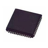
MC68HC11E1CFN3 Freescale Semiconductor, MC68HC11E1CFN3 Datasheet - Page 95

MC68HC11E1CFN3
Manufacturer Part Number
MC68HC11E1CFN3
Description
IC MCU 3MHZ 512 EEPROM 52-PLCC
Manufacturer
Freescale Semiconductor
Series
HC11r
Datasheet
1.MC68HC11E1CFN3.pdf
(268 pages)
Specifications of MC68HC11E1CFN3
Core Processor
HC11
Core Size
8-Bit
Speed
3MHz
Connectivity
SCI, SPI
Peripherals
POR, WDT
Number Of I /o
38
Program Memory Type
ROMless
Eeprom Size
512 x 8
Ram Size
512 x 8
Voltage - Supply (vcc/vdd)
4.5 V ~ 5.5 V
Data Converters
A/D 8x8b
Oscillator Type
Internal
Operating Temperature
-40°C ~ 85°C
Package / Case
52-PLCC
Data Bus Width
8 bit
Data Ram Size
512 B
Interface Type
SCI, SPI
Maximum Clock Frequency
3 MHz
Number Of Programmable I/os
22
Number Of Timers
16 bit
Maximum Operating Temperature
+ 85 C
Mounting Style
SMD/SMT
Minimum Operating Temperature
- 40 C
On-chip Adc
8 bit
Lead Free Status / RoHS Status
Contains lead / RoHS non-compliant
Program Memory Size
-
Lead Free Status / Rohs Status
Details
Available stocks
Company
Part Number
Manufacturer
Quantity
Price
Company:
Part Number:
MC68HC11E1CFN3
Manufacturer:
MOT
Quantity:
2 600
Company:
Part Number:
MC68HC11E1CFN3
Manufacturer:
MOTOROLA
Quantity:
2 337
Company:
Part Number:
MC68HC11E1CFN3
Manufacturer:
Freescale Semiconductor
Quantity:
10 000
Part Number:
MC68HC11E1CFN3
Manufacturer:
MOTOROLA/摩托罗拉
Quantity:
20 000
- Current page: 95 of 268
- Download datasheet (4Mb)
5.3.6 Computer Operating Properly (COP)
5.3.7 Serial Communications Interface (SCI)
5.3.8 Serial Peripheral Interface (SPI)
5.3.9 Analog-to-Digital (A/D) Converter
5.3.10 System
M68HC11E Family — Rev. 5
MOTOROLA
The COP watchdog system is enabled if the NOCOP control bit in the CONFIG
register is cleared and disabled if NOCOP is set. The COP rate is set for the
shortest duration timeout.
The reset condition of the SCI system is independent of the operating mode. At
reset, the SCI baud rate control register (BAUD) is initialized to $04. All transmit
and receive interrupts are masked and both the transmitter and receiver are
disabled so the port pins default to being general-purpose I/O lines. The SCI frame
format is initialized to an 8-bit character size. The send break and receiver wakeup
functions are disabled. The TDRE and TC status bits in the SCI status register
(SCSR) are both 1s, indicating that there is no transmit data in either the transmit
data register or the transmit serial shift register. The RDRF, IDLE, OR, NF, FE, PF,
and RAF receive-related status bits in the SCI control register 2 (SCCR2) are
cleared.
The SPI system is disabled by reset. The port pins associated with this function
default to being general-purpose I/O lines.
The analog-to-digital (A/D) converter configuration is indeterminate after reset. The
ADPU bit is cleared by reset, which disables the A/D system. The conversion
complete flag is indeterminate.
The EEPROM programming controls are disabled, so the memory system is
configured for normal read operation. PSEL[3:0] are initialized with the value
%0110, causing the external IRQ pin to have the highest I-bit interrupt priority. The
IRQ pin is configured for level-sensitive operation (for wired-OR systems). The
RBOOT, SMOD, and MDA bits in the HPRIO register reflect the status of the
MODB and MODA inputs at the rising edge of reset. MODA and MODB inputs
select one of the four operating modes. After reset, writing SMOD and MDA in
special modes causes the MCU to change operating modes. Refer to the
description of HPRIO register in
Memory
to specify that an oscillator startup delay is imposed upon recovery from stop
mode. The clock monitor system is disabled because CME is cleared.
Freescale Semiconductor, Inc.
For More Information On This Product,
for a detailed description of SMOD and MDA. The DLY control bit is set
Go to: www.freescale.com
Resets and Interrupts
Section 2. Operating Modes and On-Chip
Resets and Interrupts
Effects of Reset
Data Sheet
95
Related parts for MC68HC11E1CFN3
Image
Part Number
Description
Manufacturer
Datasheet
Request
R

Part Number:
Description:
MC68HC11 EEPROM Programming from a Personal Computer
Manufacturer:
Motorola / Freescale Semiconductor
Part Number:
Description:
Manufacturer:
Freescale Semiconductor, Inc
Datasheet:
Part Number:
Description:
Manufacturer:
Freescale Semiconductor, Inc
Datasheet:
Part Number:
Description:
Manufacturer:
Freescale Semiconductor, Inc
Datasheet:
Part Number:
Description:
Manufacturer:
Freescale Semiconductor, Inc
Datasheet:
Part Number:
Description:
Manufacturer:
Freescale Semiconductor, Inc
Datasheet:
Part Number:
Description:
Manufacturer:
Freescale Semiconductor, Inc
Datasheet:
Part Number:
Description:
Manufacturer:
Freescale Semiconductor, Inc
Datasheet:
Part Number:
Description:
Manufacturer:
Freescale Semiconductor, Inc
Datasheet:
Part Number:
Description:
Manufacturer:
Freescale Semiconductor, Inc
Datasheet:
Part Number:
Description:
Manufacturer:
Freescale Semiconductor, Inc
Datasheet:
Part Number:
Description:
Manufacturer:
Freescale Semiconductor, Inc
Datasheet:
Part Number:
Description:
Manufacturer:
Freescale Semiconductor, Inc
Datasheet:
Part Number:
Description:
Manufacturer:
Freescale Semiconductor, Inc
Datasheet:
Part Number:
Description:
Manufacturer:
Freescale Semiconductor, Inc
Datasheet:


