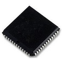
MC68HC11E0CFNE2 Freescale Semiconductor, MC68HC11E0CFNE2 Datasheet - Page 28

MC68HC11E0CFNE2
Manufacturer Part Number
MC68HC11E0CFNE2
Description
IC MCU 8BIT 2MHZ 52-PLCC
Manufacturer
Freescale Semiconductor
Series
HC11r
Specifications of MC68HC11E0CFNE2
Core Processor
HC11
Core Size
8-Bit
Speed
2MHz
Connectivity
SCI, SPI
Peripherals
POR, WDT
Number Of I /o
38
Program Memory Type
ROMless
Ram Size
512 x 8
Voltage - Supply (vcc/vdd)
4.5 V ~ 5.5 V
Data Converters
A/D 8x8b
Oscillator Type
Internal
Operating Temperature
-40°C ~ 85°C
Package / Case
52-PLCC
Controller Family/series
68HC11
No. Of I/o's
38
Ram Memory Size
512Byte
Cpu Speed
2MHz
No. Of Timers
1
Embedded Interface Type
SCI, SPI
Digital Ic Case Style
LCC
Rohs Compliant
Yes
Processor Series
HC11E
Core
HC11
Data Bus Width
8 bit
Data Ram Size
512 B
Interface Type
SCI, SPI
Maximum Clock Frequency
2 MHz
Number Of Programmable I/os
38
Number Of Timers
8
Maximum Operating Temperature
+ 85 C
Mounting Style
SMD/SMT
Minimum Operating Temperature
- 40 C
On-chip Adc
8 bit, 8 Channel
Lead Free Status / RoHS Status
Lead free / RoHS Compliant
Eeprom Size
-
Program Memory Size
-
Lead Free Status / Rohs Status
RoHS Compliant part
Electrostatic Device
Available stocks
Company
Part Number
Manufacturer
Quantity
Price
Company:
Part Number:
MC68HC11E0CFNE2
Manufacturer:
FREESCALE
Quantity:
6 221
Company:
Part Number:
MC68HC11E0CFNE2
Manufacturer:
Freescale Semiconductor
Quantity:
10 000
Company:
Part Number:
MC68HC11E0CFNE2R
Manufacturer:
Freescale Semiconductor
Quantity:
10 000
- Current page: 28 of 242
- Download datasheet (2Mb)
General Description
1.4.15 Port D
Pins PD5–PD0 can be used for general-purpose I/O signals. These pins alternately serve as the serial
communication interface (SCI) and serial peripheral interface (SPI) signals when those subsystems are
enabled.
1.4.16 Port E
Use port E for general-purpose or analog-to-digital (A/D) inputs.
28
•
•
•
PD0 is the receive data input (RxD) signal for the SCI.
PD1 is the transmit data output (TxD) signal for the SCI.
PD5–PD2 are dedicated to the SPI:
–
–
–
–
PD2 is the master in/slave out (MISO) signal.
PD3 is the master out/slave in (MOSI) signal.
PD4 is the serial clock (SCK) signal.
PD5 is the slave select (SS) input.
If high accuracy is required for A/D conversions, avoid reading port E during
sampling, as small disturbances can reduce the accuracy of that result.
M68HC11E Family Data Sheet, Rev. 5.1
CAUTION
Freescale Semiconductor
Related parts for MC68HC11E0CFNE2
Image
Part Number
Description
Manufacturer
Datasheet
Request
R

Part Number:
Description:
MC68HC11 EEPROM Programming from a Personal Computer
Manufacturer:
Motorola / Freescale Semiconductor
Part Number:
Description:
Manufacturer:
Freescale Semiconductor, Inc
Datasheet:
Part Number:
Description:
Manufacturer:
Freescale Semiconductor, Inc
Datasheet:
Part Number:
Description:
Manufacturer:
Freescale Semiconductor, Inc
Datasheet:
Part Number:
Description:
Manufacturer:
Freescale Semiconductor, Inc
Datasheet:
Part Number:
Description:
Manufacturer:
Freescale Semiconductor, Inc
Datasheet:
Part Number:
Description:
Manufacturer:
Freescale Semiconductor, Inc
Datasheet:
Part Number:
Description:
Manufacturer:
Freescale Semiconductor, Inc
Datasheet:
Part Number:
Description:
Manufacturer:
Freescale Semiconductor, Inc
Datasheet:
Part Number:
Description:
Manufacturer:
Freescale Semiconductor, Inc
Datasheet:
Part Number:
Description:
Manufacturer:
Freescale Semiconductor, Inc
Datasheet:
Part Number:
Description:
Manufacturer:
Freescale Semiconductor, Inc
Datasheet:
Part Number:
Description:
Manufacturer:
Freescale Semiconductor, Inc
Datasheet:
Part Number:
Description:
Manufacturer:
Freescale Semiconductor, Inc
Datasheet:
Part Number:
Description:
Manufacturer:
Freescale Semiconductor, Inc
Datasheet:


