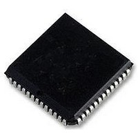
MC68HC11E0CFNE3 Freescale Semiconductor, MC68HC11E0CFNE3 Datasheet - Page 103

MC68HC11E0CFNE3
Manufacturer Part Number
MC68HC11E0CFNE3
Description
IC MCU 8BIT 3MHZ 52-PLCC
Manufacturer
Freescale Semiconductor
Series
HC11r
Specifications of MC68HC11E0CFNE3
Core Processor
HC11
Core Size
8-Bit
Speed
3MHz
Connectivity
SCI, SPI
Peripherals
POR, WDT
Number Of I /o
38
Program Memory Type
ROMless
Ram Size
512 x 8
Voltage - Supply (vcc/vdd)
4.5 V ~ 5.5 V
Data Converters
A/D 8x8b
Oscillator Type
Internal
Operating Temperature
-40°C ~ 85°C
Package / Case
52-PLCC
Controller Family/series
68HC11
No. Of I/o's
38
Ram Memory Size
512Byte
Cpu Speed
3MHz
No. Of Timers
1
Embedded Interface Type
SCI, SPI
Digital Ic Case Style
LCC
Rohs Compliant
Yes
Processor Series
HC11E
Core
HC11
Data Bus Width
8 bit
Data Ram Size
512 B
Interface Type
SCI, SPI
Maximum Clock Frequency
3 MHz
Number Of Programmable I/os
38
Number Of Timers
8
Maximum Operating Temperature
+ 85 C
Mounting Style
SMD/SMT
Minimum Operating Temperature
- 40 C
On-chip Adc
8 bit, 8 Channel
Lead Free Status / RoHS Status
Lead free / RoHS Compliant
Eeprom Size
-
Program Memory Size
-
Lead Free Status / Rohs Status
Details
Available stocks
Company
Part Number
Manufacturer
Quantity
Price
Company:
Part Number:
MC68HC11E0CFNE3
Manufacturer:
FREESCALE
Quantity:
6 249
Company:
Part Number:
MC68HC11E0CFNE3
Manufacturer:
Freescale Semiconductor
Quantity:
10 000
Company:
Part Number:
MC68HC11E0CFNE3R
Manufacturer:
Freescale Semiconductor
Quantity:
10 000
9.6.1 Pulse Accumulator Control Register
DDRA7 — Data Direction Control for Port A Bit 7
PAEN — Pulse Accumulator System Enable
PAMOD — Pulse Accumulator Mode
PEDGE — Pulse Accumulator Edge Control
DDRA3 — Data Direction Register for Port A Bit 3
I4/O5 — Input Capture 4/Output Compare 5
RTR[1:0] — RTI Interrupt Rate Selects
9.6.2 Pulse Accumulator Count Register
TECHNICAL DATA
PACTL — Pulse Accumulator Control
RESET:
Four of this register's bits control an 8-bit pulse accumulator system. Another bit en-
ables either the OC5 function or the IC4 function, while two other bits select the rate
for the real-time interrupt system.
The pulse accumulator uses port A bit 7 as the PAI input, but the pin can also be used
as general-purpose I/O or as an output compare. Note that even when port A bit 7 is
configured as an output, the pin still drives the input to the pulse accumulator. Refer to
SECTION 6 PARALLEL I/O for more information.
This bit has different meanings depending on the state of the PAMOD bit, as shown in
the following table:
Refer to SECTION 6 PARALLEL I/O.
Refer to 9.2 Input Capture.
Refer to 9.4 Real-Time Interrupt.
This 8-bit read/write register contains the count of external input events at the PAI in-
put, or the accumulated count. The counter is not affected by reset and can be read or
written at any time. Counting is synchronized to the internal PH2 clock so that incre-
menting and reading occur during opposite half cycles.
0 = Pulse accumulator disabled
1 = Pulse accumulator enabled
0 = Event counter
1 = Gated time accumulation
DDRA7
Bit 7
0
PAMOD
0
0
1
1
PAEN
Freescale Semiconductor, Inc.
6
0
For More Information On This Product,
PAMOD
PEDGE
Go to: www.freescale.com
5
0
0
1
0
1
TIMING SYSTEM
PEDGE
4
0
PAI Falling Edge Increments the Counter.
PAI Rising Edge Increments the Counter.
A Zero on PAI Inhibits Counting.
A One on PAI Inhibits Counting.
DDRA3
3
0
Action on Clock
I4/O5
2
0
RTR1
1
0
$0026
RTR0
Bit 0
0
9-17


