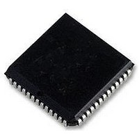
MC68HC11E0CFNE3 Freescale Semiconductor, MC68HC11E0CFNE3 Datasheet - Page 112

MC68HC11E0CFNE3
Manufacturer Part Number
MC68HC11E0CFNE3
Description
IC MCU 8BIT 3MHZ 52-PLCC
Manufacturer
Freescale Semiconductor
Series
HC11r
Specifications of MC68HC11E0CFNE3
Core Processor
HC11
Core Size
8-Bit
Speed
3MHz
Connectivity
SCI, SPI
Peripherals
POR, WDT
Number Of I /o
38
Program Memory Type
ROMless
Ram Size
512 x 8
Voltage - Supply (vcc/vdd)
4.5 V ~ 5.5 V
Data Converters
A/D 8x8b
Oscillator Type
Internal
Operating Temperature
-40°C ~ 85°C
Package / Case
52-PLCC
Controller Family/series
68HC11
No. Of I/o's
38
Ram Memory Size
512Byte
Cpu Speed
3MHz
No. Of Timers
1
Embedded Interface Type
SCI, SPI
Digital Ic Case Style
LCC
Rohs Compliant
Yes
Processor Series
HC11E
Core
HC11
Data Bus Width
8 bit
Data Ram Size
512 B
Interface Type
SCI, SPI
Maximum Clock Frequency
3 MHz
Number Of Programmable I/os
38
Number Of Timers
8
Maximum Operating Temperature
+ 85 C
Mounting Style
SMD/SMT
Minimum Operating Temperature
- 40 C
On-chip Adc
8 bit, 8 Channel
Lead Free Status / RoHS Status
Lead free / RoHS Compliant
Eeprom Size
-
Program Memory Size
-
Lead Free Status / Rohs Status
Details
Available stocks
Company
Part Number
Manufacturer
Quantity
Price
Company:
Part Number:
MC68HC11E0CFNE3
Manufacturer:
FREESCALE
Quantity:
6 249
Company:
Part Number:
MC68HC11E0CFNE3
Manufacturer:
Freescale Semiconductor
Quantity:
10 000
Company:
Part Number:
MC68HC11E0CFNE3R
Manufacturer:
Freescale Semiconductor
Quantity:
10 000
A-8
NOTES:
Frequency of Operation (E-Clock Frequency)
E-Clock Period
Peripheral Data Setup Time
Peripheral Data Hold Time
Delay Time, Peripheral Data Write
MCU Read of Ports A, B, C, and D
MCU Read of Ports A, B, C, and D
MCU Write to Port A
MCU Writes to Ports B, C, and D
t
1. Port C and D timing is valid for active drive (CWOM and DWOM bits not set in PIOC and SPCR registers respec-
2. All timing is shown with respect to 20% V
PWD
A, B, C, D
tively).
PORT A
PORTS
B, C, D
PORTS
= 1/4 t
E
E
cyc
+ 150 ns
Characteristic
PREVIOUS PORT DATA
Freescale Semiconductor, Inc.
Figure A-6 Port Write Timing Diagram
Figure A-7 Port Read Timing Diagram
For More Information On This Product,
Table A-5 Peripheral Port Timing
ELECTRICAL CHARACTERISTICS
MCU WRITE TO PORT
PREVIOUS PORT DATA
MCU READ OF PORT
Go to: www.freescale.com
DD
and 70% V
Symbol
t
t
PDSU
t
PWD
t
PDH
cyc
f
t PWD
o
DD
1000
, unless otherwise noted.
Min
100
dc
50
—
—
1.0 MHz
t PDSU
Max
200
350
1.0
—
—
—
Min
500
100
NEW DATA VALID
t PWD
50
dc
—
—
t PDH
2.0 MHz
Max
200
225
2.0
—
—
—
NEW DATA VALID
TECHNICAL DATA
Min
333
100
dc
50
—
—
3.0 MHz
D3 PORT WRITE TIM
Max
D3 PORT READ TIM
200
183
3.0
—
—
—
MHz
Unit
ns
ns
ns
ns
ns


