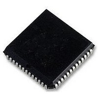
MC68HC11E0CFNE3 Freescale Semiconductor, MC68HC11E0CFNE3 Datasheet - Page 36

MC68HC11E0CFNE3
Manufacturer Part Number
MC68HC11E0CFNE3
Description
IC MCU 8BIT 3MHZ 52-PLCC
Manufacturer
Freescale Semiconductor
Series
HC11r
Specifications of MC68HC11E0CFNE3
Core Processor
HC11
Core Size
8-Bit
Speed
3MHz
Connectivity
SCI, SPI
Peripherals
POR, WDT
Number Of I /o
38
Program Memory Type
ROMless
Ram Size
512 x 8
Voltage - Supply (vcc/vdd)
4.5 V ~ 5.5 V
Data Converters
A/D 8x8b
Oscillator Type
Internal
Operating Temperature
-40°C ~ 85°C
Package / Case
52-PLCC
Controller Family/series
68HC11
No. Of I/o's
38
Ram Memory Size
512Byte
Cpu Speed
3MHz
No. Of Timers
1
Embedded Interface Type
SCI, SPI
Digital Ic Case Style
LCC
Rohs Compliant
Yes
Processor Series
HC11E
Core
HC11
Data Bus Width
8 bit
Data Ram Size
512 B
Interface Type
SCI, SPI
Maximum Clock Frequency
3 MHz
Number Of Programmable I/os
38
Number Of Timers
8
Maximum Operating Temperature
+ 85 C
Mounting Style
SMD/SMT
Minimum Operating Temperature
- 40 C
On-chip Adc
8 bit, 8 Channel
Lead Free Status / RoHS Status
Lead free / RoHS Compliant
Eeprom Size
-
Program Memory Size
-
Lead Free Status / Rohs Status
Details
Available stocks
Company
Part Number
Manufacturer
Quantity
Price
Company:
Part Number:
MC68HC11E0CFNE3
Manufacturer:
FREESCALE
Quantity:
6 249
Company:
Part Number:
MC68HC11E0CFNE3
Manufacturer:
Freescale Semiconductor
Quantity:
10 000
Company:
Part Number:
MC68HC11E0CFNE3R
Manufacturer:
Freescale Semiconductor
Quantity:
10 000
4.1.3 Special Test Mode
4.1.4 Bootstrap Mode
4-2
Special test, a variation of the expanded multiplexed mode, is primarily used during
Motorola's internal production testing; however, it is accessible for programming the
CONFIG register, and supporting emulation and debugging during development.
When the MCU is reset in special bootstrap mode, a small amount of on-chip ROM is
enabled at address $BF00–$BFFF. The ROM contains a bootloader program and a
special set of interrupt and reset vectors. The MCU fetches the reset vector, then ex-
ecutes the bootloader.
For normal use of the bootloader program, send $FF to the SCI receiver at either E
clock 16, or E clock 104 (1200 baud for E clock equals 2 MHz). Then download up
to 192 bytes of program data, which is put into RAM starting at $0040. These charac-
ters are echoed through the transmitter. When loading is complete, the program jumps
to location $0040 and begins executing the code. The bootloader program ends the
download after 192 bytes, or when the received data line is idle for at least four char-
acter times. Use of an external pullup resistor is required when using the SCI transmit-
ter pin because port D pins are configured for wired-OR operation by the bootloader.
In bootstrap mode, the interrupt vectors are directed to RAM. This allows the use of
interrupts through a jump table. Refer to Freescale application note AN1060,
MC68HC11 Bootstrap Mode.
MCU
PB7
PB6
PB5
PB4
PB3
PB2
PB1
PB0
PC7
PC6
PC5
PC4
PC3
PC2
PC1
PC0
R/W
AS
E
Figure 4-1 Address/Data Demultiplexing
Freescale Semiconductor, Inc.
OPERATING MODES AND ON-CHIP MEMORY
For More Information On This Product,
Go to: www.freescale.com
D1
D2
D3
D4
D5
D6
D7
D8
LE
HC373
OE
Q1
Q2
Q3
Q4
Q5
Q6
Q7
Q8
ADDR15
ADDR14
ADDR13
ADDR12
ADDR11
ADDR10
ADDR9
ADDR8
ADDR7
ADDR6
ADDR5
ADDR4
ADDR3
ADDR2
ADDR1
ADDR0
WE
OE
DATA7
DATA6
DATA5
DATA4
DATA3
DATA2
DATA1
DATA0
ADDR/DATA DEMUX
TECHNICAL DATA


