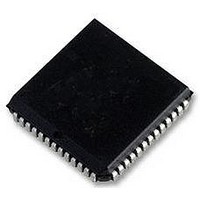
MC68HC11E0CFNE3 Freescale Semiconductor, MC68HC11E0CFNE3 Datasheet - Page 89

MC68HC11E0CFNE3
Manufacturer Part Number
MC68HC11E0CFNE3
Description
IC MCU 8BIT 3MHZ 52-PLCC
Manufacturer
Freescale Semiconductor
Series
HC11r
Specifications of MC68HC11E0CFNE3
Core Processor
HC11
Core Size
8-Bit
Speed
3MHz
Connectivity
SCI, SPI
Peripherals
POR, WDT
Number Of I /o
38
Program Memory Type
ROMless
Ram Size
512 x 8
Voltage - Supply (vcc/vdd)
4.5 V ~ 5.5 V
Data Converters
A/D 8x8b
Oscillator Type
Internal
Operating Temperature
-40°C ~ 85°C
Package / Case
52-PLCC
Controller Family/series
68HC11
No. Of I/o's
38
Ram Memory Size
512Byte
Cpu Speed
3MHz
No. Of Timers
1
Embedded Interface Type
SCI, SPI
Digital Ic Case Style
LCC
Rohs Compliant
Yes
Processor Series
HC11E
Core
HC11
Data Bus Width
8 bit
Data Ram Size
512 B
Interface Type
SCI, SPI
Maximum Clock Frequency
3 MHz
Number Of Programmable I/os
38
Number Of Timers
8
Maximum Operating Temperature
+ 85 C
Mounting Style
SMD/SMT
Minimum Operating Temperature
- 40 C
On-chip Adc
8 bit, 8 Channel
Lead Free Status / RoHS Status
Lead free / RoHS Compliant
Eeprom Size
-
Program Memory Size
-
Lead Free Status / Rohs Status
Details
Available stocks
Company
Part Number
Manufacturer
Quantity
Price
Company:
Part Number:
MC68HC11E0CFNE3
Manufacturer:
FREESCALE
Quantity:
6 249
Company:
Part Number:
MC68HC11E0CFNE3
Manufacturer:
Freescale Semiconductor
Quantity:
10 000
Company:
Part Number:
MC68HC11E0CFNE3R
Manufacturer:
Freescale Semiconductor
Quantity:
10 000
9.1 Timer Structure
TECHNICAL DATA
Figure 9-1 shows the capture/compare system block diagram. The port A pin control
block includes logic for timer functions and for general-purpose I/O. For pins PA2,
PA1, and PA0, this block contains both the edge-detection logic and the control logic
that enables the selection of which edge triggers an input capture. The digital level on
PA[2:0] can be read at any time (read PORTA register), even if the pin is being used
for the input capture function. Pins PA[6:4] are used for either general-purpose output,
or as output compare pins. Pin PA3 can be used for general-purpose I/O, input capture
4, output compare 5, or output compare 1. When one of these pins is being used for
an output compare function, it cannot be written directly as if it were a general-purpose
output. Each of the output compare functions (OC5–OC2) is related to one of the port
A output pins. Output compare one (OC1) has extra control logic, allowing it optional
control of any combination of the PA[7:3] pins. The PA7 pin can be used as a general-
purpose I/O pin, as an input to the pulse accumulator, or as an OC1 output pin.
overflow —
overflow —
overflow —
overflow —
1 count —
1 count —
1 count —
1 count —
Control
PR[1:0]
Bits
0 0
0 1
1 0
1 1
Freescale Semiconductor, Inc.
For More Information On This Product,
65.536 ms
262.14 ms
524.29 ms
4.0 MHz
1.0 MHz
1000 ns
16.0 µs
1.049 s
1.0 µs
4.0 µs
8.0 µs
Table 9-1 Timer Summary
Go to: www.freescale.com
TIMING SYSTEM
XTAL Frequencies
32.768 ms
131.07 ms
262.14 ms
524.29 ms
8.0 MHz
2.0 MHz
500 ns
Main Timer Count Rates
500 ns
2.0 µs
4.0 µs
8.0 µs
21.845 ms
87.381 ms
174.76 ms
349.52 ms
12.0 MHz
1.333 µs
2.667 µs
5.333 µs
3.0 MHz
333 ns
333 ns
Other Rates
(E/2
(E/2
(E/2
(E/2
(E/16)
(1/E)
(E/1)
(E/4)
(E/8)
(E)
16
18
19
20
)
)
)
)
9-3


