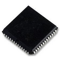
MC68HC11E0CFNE3 Freescale Semiconductor, MC68HC11E0CFNE3 Datasheet - Page 92

MC68HC11E0CFNE3
Manufacturer Part Number
MC68HC11E0CFNE3
Description
IC MCU 8BIT 3MHZ 52-PLCC
Manufacturer
Freescale Semiconductor
Series
HC11r
Specifications of MC68HC11E0CFNE3
Core Processor
HC11
Core Size
8-Bit
Speed
3MHz
Connectivity
SCI, SPI
Peripherals
POR, WDT
Number Of I /o
38
Program Memory Type
ROMless
Ram Size
512 x 8
Voltage - Supply (vcc/vdd)
4.5 V ~ 5.5 V
Data Converters
A/D 8x8b
Oscillator Type
Internal
Operating Temperature
-40°C ~ 85°C
Package / Case
52-PLCC
Controller Family/series
68HC11
No. Of I/o's
38
Ram Memory Size
512Byte
Cpu Speed
3MHz
No. Of Timers
1
Embedded Interface Type
SCI, SPI
Digital Ic Case Style
LCC
Rohs Compliant
Yes
Processor Series
HC11E
Core
HC11
Data Bus Width
8 bit
Data Ram Size
512 B
Interface Type
SCI, SPI
Maximum Clock Frequency
3 MHz
Number Of Programmable I/os
38
Number Of Timers
8
Maximum Operating Temperature
+ 85 C
Mounting Style
SMD/SMT
Minimum Operating Temperature
- 40 C
On-chip Adc
8 bit, 8 Channel
Lead Free Status / RoHS Status
Lead free / RoHS Compliant
Eeprom Size
-
Program Memory Size
-
Lead Free Status / Rohs Status
Details
Available stocks
Company
Part Number
Manufacturer
Quantity
Price
Company:
Part Number:
MC68HC11E0CFNE3
Manufacturer:
FREESCALE
Quantity:
6 249
Company:
Part Number:
MC68HC11E0CFNE3
Manufacturer:
Freescale Semiconductor
Quantity:
10 000
Company:
Part Number:
MC68HC11E0CFNE3R
Manufacturer:
Freescale Semiconductor
Quantity:
10 000
TI4/O5 — Timer Input Capture 4/Output Compare 5
9.2.2 Timer Input Capture Registers
9.2.3 Timer Input Capture 4/Output Compare 5 Register
9.3 Output Compare
9-6
TIC1–TIC3 — Timer Input Capture
RESET:
RESET:
$001E
$001F
$0010
$0011
$0012
$0013
$0014
$0015
When an edge has been detected and synchronized, the 16-bit free-running counter
value is transferred into the input capture register pair as a single 16-bit parallel trans-
fer. Timer counter value captures and timer counter incrementing occur on opposite
half-cycles of the phase two clock so that the count value is stable whenever a capture
occurs. The TICx registers are not affected by reset. Input capture values can be read
from a pair of 8-bit read-only registers. A read of the high-order byte of an input capture
register pair inhibits a new capture transfer for one bus cycle. If a double-byte read in-
struction, such as LDD, is used to read the captured value, coherency is assured.
When a new input capture occurs immediately after a high-order byte read, transfer is
delayed for an additional cycle but the value is not lost.
Use TI4/O5 as either an input capture register or an output compare register, depend-
ing on the function chosen for the I4/O5 pin. To enable it as an input capture pin, set
the I4/O5 bit in the pulse accumulator control register (PACTL) to logic level one. To
use it as an output compare register, set the I4/O5 bit to a logic level zero. Refer to 9.6
Pulse Accumulator.
Use the output compare (OC) function to program an action to occur at a specific time
— when the 16-bit counter reaches a specified value. For each of the five output com-
pare functions, there is a separate 16-bit compare register and a dedicated 16-bit com-
parator. The value in the compare register is compared to the value of the free-running
counter on every bus cycle. When the compare register matches the counter value, an
output compare status flag is set. The flag can be used to initiate the automatic actions
for that output compare function.
To produce a pulse of a specific duration, write to the output compare register a value
representing the time the leading edge of the pulse is to occur. The output compare
circuit is configured to set the appropriate output either high or low, depending on the
Bit 15
Bit 15
Bit 15
Bit 7
Bit 7
Bit 7
Bit 15
Bit 7
14
14
14
6
6
6
14
6
Freescale Semiconductor, Inc.
For More Information On This Product,
13
13
13
5
5
5
13
5
All I4/O5 register pairs reset to ones ($FFFF).
Input capture registers not affected by reset.
Go to: www.freescale.com
TIMING SYSTEM
12
12
12
4
4
4
12
4
11
11
11
3
3
3
11
3
10
10
10
10
2
2
2
2
9
1
9
1
9
1
9
1
Bit 8
Bit 0
Bit 8
Bit 0
Bit 8
Bit 0
Bit 8
Bit 0
TECHNICAL DATA
$001E, $001F
$0010–$0015
TI4/O5 (High)
TI4/O5 (Low)
TIC1 (High)
TIC2 (High)
TIC3 (High)
TIC1 (Low)
TIC2 (Low)
TIC3 (Low)


