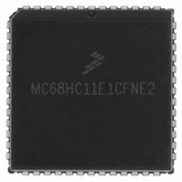
MC68HC11E1CFNE2 Freescale Semiconductor, MC68HC11E1CFNE2 Datasheet - Page 101

MC68HC11E1CFNE2
Manufacturer Part Number
MC68HC11E1CFNE2
Description
IC MCU 8BIT 3MHZ 52-PLCC
Manufacturer
Freescale Semiconductor
Series
HC11r
Specifications of MC68HC11E1CFNE2
Core Processor
HC11
Core Size
8-Bit
Speed
3MHz
Connectivity
SCI, SPI
Peripherals
POR, WDT
Number Of I /o
38
Program Memory Type
ROMless
Eeprom Size
512 x 8
Ram Size
512 x 8
Voltage - Supply (vcc/vdd)
4.5 V ~ 5.5 V
Data Converters
A/D 8x8b
Oscillator Type
Internal
Operating Temperature
-40°C ~ 85°C
Package / Case
52-PLCC
A/d Inputs
8-Channel, 8-Bit
Eeprom Memory
512 Bytes
Input Output
38
Interface
SCI/SPI
Memory Type
ROM
Number Of Bits
8
Package Type
52-pin PLCC
Programmable Memory
0 Bytes
Timers
3-16-bit
Voltage, Range
3-5.5 V
Controller Family/series
68HC11
No. Of I/o's
38
Eeprom Memory Size
512Byte
Ram Memory Size
512Byte
Cpu Speed
2MHz
No. Of Timers
1
Embedded Interface Type
SCI, SPI
Rohs Compliant
Yes
Processor Series
HC11E
Core
HC11
Data Bus Width
8 bit
Data Ram Size
512 B
Interface Type
SCI, SPI
Maximum Clock Frequency
2 MHz
Number Of Programmable I/os
38
Number Of Timers
8
Maximum Operating Temperature
+ 85 C
Mounting Style
SMD/SMT
Minimum Operating Temperature
- 40 C
On-chip Adc
8 bit, 8 Channel
Lead Free Status / RoHS Status
Lead free / RoHS Compliant
Program Memory Size
-
Lead Free Status / Rohs Status
RoHS Compliant part
Available stocks
Company
Part Number
Manufacturer
Quantity
Price
Company:
Part Number:
MC68HC11E1CFNE2
Manufacturer:
Phoenix
Quantity:
2 000
Company:
Part Number:
MC68HC11E1CFNE2
Manufacturer:
Freescale Semiconductor
Quantity:
10 000
Part Number:
MC68HC11E1CFNE2
Manufacturer:
FREESCALE
Quantity:
20 000
Company:
Part Number:
MC68HC11E1CFNE2R
Manufacturer:
Freescale Semiconductor
Quantity:
10 000
Company:
Part Number:
MC68HC11E1CFNE2R2
Manufacturer:
FREESCALE
Quantity:
5 510
Company:
Part Number:
MC68HC11E1CFNE2R2
Manufacturer:
MICROCHIP
Quantity:
5 510
6.6 Port E
Port E is used for general-purpose static inputs or pins that share functions with the analog-to-digital (A/D)
converter system. When some port E pins are being used for general-purpose input and others are being
used as A/D inputs, PORTE should not be read during the sample portion of an A/D conversion.
6.7 Handshake Protocol
Simple and full handshake input and output functions are available on ports B and C pins in single-chip
mode. In simple strobed mode, port B is a strobed output port and port C is a latching input port. The two
activities are available simultaneously.
The STRB output is pulsed for two E-clock periods each time there is a write to the PORTB register. The
INVB bit in the PIOC register controls the polarity of STRB pulses. Port C levels are latched into the
alternate port C latch (PORTCL) register on each assertion of the STRA input. STRA edge select, flag,
and interrupt enable bits are located in the PIOC register. Any or all of the port C lines can still be used
as general-purpose I/O while in strobed input mode.
Full handshake modes use port C pins and the STRA and STRB lines. Input and output handshake
modes are supported, and output handshake mode has a 3-stated variation. STRA is an edge-detecting
input and STRB is a handshake output. Control and enable bits are located in the PIOC register.
In full input handshake mode, the MCU asserts STRB to signal an external system that it is ready to latch
data. Port C logic levels are latched into PORTCL when the STRA line is asserted by the external system.
The MCU then negates STRB. The MCU reasserts STRB after the PORTCL register is read. In this mode,
a mix of latched inputs, static inputs, and static outputs is allowed on port C, differentiated by the data
direction bits and use of the PORTC and PORTCL registers.
In full output handshake mode, the MCU writes data to PORTCL which, in turn, asserts the STRB output
to indicate that data is ready. The external system reads port C data and asserts the STRA input to
acknowledge that data has been received.
In the 3-state variation of output handshake mode, lines intended as 3-state handshake outputs are
configured as inputs by clearing the corresponding DDRC bits. The MCU writes data to PORTCL and
asserts STRB. The external system responds by activating the STRA input, which forces the MCU to drive
the data in PORTC out on all of the port C lines. After the trailing edge of the active signal on STRA, the
MCU negates the STRB signal. The 3-state mode variation does not allow part of port C to be used for
static inputs while other port C pins are being used for handshake outputs. Refer to the
Control Register
Freescale Semiconductor
Alternate Function:
for further information.
Address:
Reset:
Read:
Write:
$100A
Bit 7
PE7
AN7
Figure 6-9. Port E Data Register (PORTE)
M68HC11E Family Data Sheet, Rev. 5.1
PE6
AN6
6
PE5
AN5
5
Indeterminate after reset
PE4
AN4
4
AN3
PE3
3
AN2
PE2
2
AN1
PE1
1
6.8 Parallel I/O
Bit 0
PE0
AN0
Port E
101


