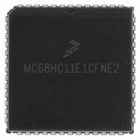
MC68HC11E1CFNE2 Freescale Semiconductor, MC68HC11E1CFNE2 Datasheet - Page 62

MC68HC11E1CFNE2
Manufacturer Part Number
MC68HC11E1CFNE2
Description
IC MCU 8BIT 3MHZ 52-PLCC
Manufacturer
Freescale Semiconductor
Series
HC11r
Specifications of MC68HC11E1CFNE2
Core Processor
HC11
Core Size
8-Bit
Speed
3MHz
Connectivity
SCI, SPI
Peripherals
POR, WDT
Number Of I /o
38
Program Memory Type
ROMless
Eeprom Size
512 x 8
Ram Size
512 x 8
Voltage - Supply (vcc/vdd)
4.5 V ~ 5.5 V
Data Converters
A/D 8x8b
Oscillator Type
Internal
Operating Temperature
-40°C ~ 85°C
Package / Case
52-PLCC
A/d Inputs
8-Channel, 8-Bit
Eeprom Memory
512 Bytes
Input Output
38
Interface
SCI/SPI
Memory Type
ROM
Number Of Bits
8
Package Type
52-pin PLCC
Programmable Memory
0 Bytes
Timers
3-16-bit
Voltage, Range
3-5.5 V
Controller Family/series
68HC11
No. Of I/o's
38
Eeprom Memory Size
512Byte
Ram Memory Size
512Byte
Cpu Speed
2MHz
No. Of Timers
1
Embedded Interface Type
SCI, SPI
Rohs Compliant
Yes
Processor Series
HC11E
Core
HC11
Data Bus Width
8 bit
Data Ram Size
512 B
Interface Type
SCI, SPI
Maximum Clock Frequency
2 MHz
Number Of Programmable I/os
38
Number Of Timers
8
Maximum Operating Temperature
+ 85 C
Mounting Style
SMD/SMT
Minimum Operating Temperature
- 40 C
On-chip Adc
8 bit, 8 Channel
Lead Free Status / RoHS Status
Lead free / RoHS Compliant
Program Memory Size
-
Lead Free Status / Rohs Status
RoHS Compliant part
Available stocks
Company
Part Number
Manufacturer
Quantity
Price
Company:
Part Number:
MC68HC11E1CFNE2
Manufacturer:
Phoenix
Quantity:
2 000
Company:
Part Number:
MC68HC11E1CFNE2
Manufacturer:
Freescale Semiconductor
Quantity:
10 000
Part Number:
MC68HC11E1CFNE2
Manufacturer:
FREESCALE
Quantity:
20 000
Company:
Part Number:
MC68HC11E1CFNE2R
Manufacturer:
Freescale Semiconductor
Quantity:
10 000
Company:
Part Number:
MC68HC11E1CFNE2R2
Manufacturer:
FREESCALE
Quantity:
5 510
Company:
Part Number:
MC68HC11E1CFNE2R2
Manufacturer:
MICROCHIP
Quantity:
5 510
Analog-to-Digital (A/D) Converter
3.7 Multiple-Channel Operation
The two types of multiple-channel operation are:
3.8 Operation in Stop and Wait Modes
If a conversion sequence is in progress when either the stop or wait mode is entered, the conversion of
the current channel is suspended. When the MCU resumes normal operation, that channel is resampled
and the conversion sequence is resumed. As the MCU exits wait mode, the A/D circuits are stable and
valid results can be obtained on the first conversion. However, in stop mode, all analog bias currents are
disabled and it is necessary to allow a stabilization period when leaving stop mode. If stop mode is exited
with a delay (DLY = 1), there is enough time for these circuits to stabilize before the first conversion. If
stop mode is exited with no delay (DLY bit in OPTION register = 0), allow 10 ms for the A/D circuitry to
stabilize to avoid invalid results.
3.9 A/D Control/Status Register
All bits in this register can be read or written, except bit 7, which is a read-only status indicator, and bit 6,
which always reads as 0. Write to ADCTL to initiate a conversion. To quit a conversion in progress, write
to this register and a new conversion sequence begins immediately.
CCF — Conversion Complete Flag
Bit 6 — Unimplemented
SCAN — Continuous Scan Control Bit
62
1. When SCAN = 0, a selected group of four channels is converted one time each. The first result is
2. When SCAN = 1, conversions continue to be performed on the selected group of channels with the
A read-only status indicator, this bit is set when all four A/D result registers contain valid conversion
results. Each time the ADCTL register is overwritten, this bit is automatically cleared to 0 and a
conversion sequence is started. In the continuous mode, CCF is set at the end of the first conversion
sequence.
Always reads 0
stored in A/D result register 1 (ADR1), and the fourth result is stored in ADR4. After the fourth
conversion is complete, all conversion activity is halted until a new conversion command is written
to the ADCTL register.
fifth conversion being stored in register ADR1 (replacing the earlier conversion result for the first
channel in the group), the sixth conversion overwriting ADR2, and so on.
Address: $1030
Reset:
Read:
Write:
CCF
Bit 7
0
Figure 3-5. A/D Control/Status Register (ADCTL)
= Unimplemented
6
0
M68HC11E Family Data Sheet, Rev. 5.1
SCAN
5
MULT
4
Indeterminate after reset
CD
3
CC
2
CB
1
Freescale Semiconductor
Bit 0
CA


