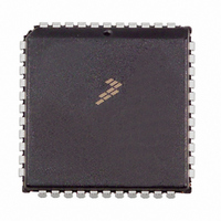
MC68HC711D3CFNE2 Freescale Semiconductor, MC68HC711D3CFNE2 Datasheet - Page 49

MC68HC711D3CFNE2
Manufacturer Part Number
MC68HC711D3CFNE2
Description
IC MCU 8BIT 3MHZ 44-PLCC
Manufacturer
Freescale Semiconductor
Series
HC11r
Specifications of MC68HC711D3CFNE2
Core Processor
HC11
Core Size
8-Bit
Speed
2MHz
Connectivity
SCI, SPI
Peripherals
POR, WDT
Number Of I /o
26
Program Memory Size
4KB (4K x 8)
Program Memory Type
OTP
Ram Size
192 x 8
Voltage - Supply (vcc/vdd)
4.5 V ~ 5.5 V
Oscillator Type
Internal
Operating Temperature
-40°C ~ 85°C
Package / Case
44-PLCC
Lead Free Status / RoHS Status
Lead free / RoHS Compliant
Eeprom Size
-
Data Converters
-
Available stocks
Company
Part Number
Manufacturer
Quantity
Price
Company:
Part Number:
MC68HC711D3CFNE2
Manufacturer:
ALLEGEO
Quantity:
4 492
Company:
Part Number:
MC68HC711D3CFNE2
Manufacturer:
Freescale Semiconductor
Quantity:
10 000
5.2.3 Parallel I/O
5.2.4 Timer
5.2.5 Real-Time Interrupt
5.2.6 Pulse Accumulator
TECHNICAL DATA
When a reset occurs in expanded multiplexed operating modes, the pins used for par-
allel I/O are dedicated to the expansion bus. In single-chip and bootstrap modes, all
ports are parallel I/O data ports. In expanded multiplexed and test modes, ports B, C,
and lines DATA6/AS and DATA7/R/W are a memory expansion bus with port B as a
high-order address bus, port C as a multiplexed address and data bus, AS as the de-
multiplexing signal, and R/as the data bus direction control. The CWOM bit in PIOC is
cleared so that port C is not in wired-OR mode. Port A, bits [0:3] and 7; and ports B,
C, and D are general-purpose I/O at reset and set for input. For this reason the pins
are configured as high impedance upon reset. Port A bits [4:6] are outputs, so high im-
pedance protection is not necessary.
During reset, the timing system is initialized to a count of $0000. The prescaler bits are
cleared, and all output compare registers are initialized to $FFFF. All input capture reg-
isters are indeterminate after reset. The output compare 1 mask (OC1M) register is
cleared so that successful OC1 compares do not affect any I/O pins. The other four
output compares are configured so that they do not affect any I/O pins on successful
compares. All input capture edge-detector circuits are configured for capture disabled
operation. The timer overflow interrupt flag and all eight timer function interrupt flags
are cleared. All nine timer interrupts are disabled because their mask bits have been
cleared.
The I4/O5 bit in the PACTL register is cleared to configure the I4/O5 function as OC5;
however, the OM5:OL5 control bits in the TCTL1 register are clear so OC5 does not
control the PA3 pin.
The real-time interrupt flag (RTIF) is cleared and automatic hardware interrupts are
masked. The rate control bits are cleared after reset and can be initialized by software
before the real-time interrupt (RTI) system is used. After reset, a full RTI period elaps-
es before the first RTI interrupt.
The pulse accumulator system is disabled at reset so that the PAI input pin defaults to
being a general-purpose input pin (PA7).
Do not confuse pin function with the electrical state of the pin at reset.
All general-purpose I/O pins configured as inputs at reset are in a
high impedance state. Port data registers reflect the port's functional
state at reset. The pin function is mode dependent.
Freescale Semiconductor, Inc.
For More Information On This Product,
RESETS AND INTERRUPTS
Go to: www.freescale.com
NOTE
5-5


