R5F21274SYFP#U0 Renesas Electronics America, R5F21274SYFP#U0 Datasheet - Page 13
R5F21274SYFP#U0
Manufacturer Part Number
R5F21274SYFP#U0
Description
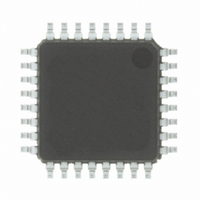
IC R8C/27 MCU FLASH 32LQFP
Manufacturer
Renesas Electronics America
Series
R8C/2x/27r
Datasheet
1.R5F21276SNFPU0.pdf
(75 pages)
Specifications of R5F21274SYFP#U0
Core Processor
R8C
Core Size
16/32-Bit
Speed
20MHz
Connectivity
I²C, LIN, SIO, SSU, UART/USART
Peripherals
LED, POR, Voltage Detect, WDT
Number Of I /o
25
Program Memory Size
16KB (16K x 8)
Program Memory Type
FLASH
Ram Size
1K x 8
Voltage - Supply (vcc/vdd)
2.2 V ~ 5.5 V
Data Converters
A/D 12x10b
Oscillator Type
Internal
Operating Temperature
-20°C ~ 105°C
Package / Case
32-LQFP
For Use With
R0E521000EPB00 - PROBE EMULATOR FOR PC7501
Lead Free Status / RoHS Status
Lead free / RoHS Compliant
Eeprom Size
-
Available stocks
Company
Part Number
Manufacturer
Quantity
Price

Part Number:
R5F21274SYFP#U0R5F21274SYFP#V0
Manufacturer:
Renesas Electronics America
Quantity:
10 000
Part Number:
R5F21274SYFP#U0R5F21274SYFP#V2
Manufacturer:
Renesas Electronics America
Quantity:
10 000


R8C/26 Group, R8C/27 Group
Rev.2.10
REJ03B0168-0210
Table 1.6
NOTES:
Number
Pin
1. This can be assigned to the pin in parentheses by a program.
2. XCIN, XCOUT can be used only for N or D version.
3. For the combination of using pins TXD1 and RXD1, refer to Figure 15.7 Registers PINSR1 and
10
12
13
14
15
16
17
18
19
20
21
22
23
24
25
26
27
28
29
30
31
32
11
1
2
3
4
5
6
7
8
9
PMR of Hardware Manual (REJ09B0278).
Sep 26, 2008
XOUT/XCOUT
XIN/XCIN
VCC/AVCC
Control Pin
VSS/AVSS
RESET
MODE
Pin Name Information by Pin Number
VRFF
(2)
(2)
Page 11 of 69
P3_5
P3_7
P4_7
P4_6
P4_5
P1_7
P3_6
P3_1
P5_4
P5_3
P1_6
P1_5
P1_4
P1_3
P1_2
P4_2
P1_1
P1_0
P3_3
P3_4
P0_7
P0_6
P0_5
P0_4
P0_3
P0_2
P0_1
P0_0
Port
(INT1)
(INT1)
Interrupt
INT0
INT1
INT3
KI3
KI2
KI1
KI0
(1)
(1)
(TRCIOD)
(TRCIOC)
(TRAIO)
TRCTRG
TRCIOA/
TRCCLK
TRCIOD
TRCIOC
TRCIOB
(TRBO)
TRAIO
TRAO
TRBO
TREO
Timer
I/O Pin Functions for of Peripheral Modules
(1)
(1)
(1)
(RXD1)
(RXD1)
(TXD1)
(TXD1)
Interface
(TXD1)/
RXD1/
RXD0
Serial
CLK0
TXD0
CLK1
(1, 3)
(1, 3)
(1, 3)
(1, 3)
Serial I/O with
Synchronous
Chip Select
(SSI)
SSCK
Clock
SSO
SCS
SSI
(1)
Interface
I
2
SDA
SCL
C bus
Converter
1. Overview
AN11
AN10
AN9
AN8
AN0
AN1
AN2
AN3
AN4
AN5
AN6
AN7
A/D
Related parts for R5F21274SYFP#U0
Image
Part Number
Description
Manufacturer
Datasheet
Request
R

Part Number:
Description:
KIT STARTER FOR M16C/29
Manufacturer:
Renesas Electronics America
Datasheet:

Part Number:
Description:
KIT STARTER FOR R8C/2D
Manufacturer:
Renesas Electronics America
Datasheet:

Part Number:
Description:
R0K33062P STARTER KIT
Manufacturer:
Renesas Electronics America
Datasheet:

Part Number:
Description:
KIT STARTER FOR R8C/23 E8A
Manufacturer:
Renesas Electronics America
Datasheet:

Part Number:
Description:
KIT STARTER FOR R8C/25
Manufacturer:
Renesas Electronics America
Datasheet:

Part Number:
Description:
KIT STARTER H8S2456 SHARPE DSPLY
Manufacturer:
Renesas Electronics America
Datasheet:

Part Number:
Description:
KIT STARTER FOR R8C38C
Manufacturer:
Renesas Electronics America
Datasheet:

Part Number:
Description:
KIT STARTER FOR R8C35C
Manufacturer:
Renesas Electronics America
Datasheet:

Part Number:
Description:
KIT STARTER FOR R8CL3AC+LCD APPS
Manufacturer:
Renesas Electronics America
Datasheet:
Part Number:
Description:
KIT STARTER FOR RX610
Manufacturer:
Renesas Electronics America
Datasheet:

Part Number:
Description:
KIT STARTER FOR R32C/118
Manufacturer:
Renesas Electronics America
Datasheet:

Part Number:
Description:
KIT DEV RSK-R8C/26-29
Manufacturer:
Renesas Electronics America
Datasheet:

Part Number:
Description:
KIT STARTER FOR SH7124
Manufacturer:
Renesas Electronics America
Datasheet:

Part Number:
Description:
KIT STARTER FOR H8SX/1622
Manufacturer:
Renesas Electronics America
Datasheet:

Part Number:
Description:
KIT DEV FOR SH7203
Manufacturer:
Renesas Electronics America
Datasheet: