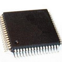
SAK-C164CM-4EF AB Infineon Technologies, SAK-C164CM-4EF AB Datasheet - Page 9

SAK-C164CM-4EF AB
Manufacturer Part Number
SAK-C164CM-4EF AB
Description
IC MCU 16BIT 32KB OTP TQFP-64-4
Manufacturer
Infineon Technologies
Series
C16xxr
Datasheet
1.SAF-C164CM-4EF_AB.pdf
(68 pages)
Specifications of SAK-C164CM-4EF AB
Core Processor
C166
Core Size
16-Bit
Speed
20MHz
Connectivity
CAN, EBI/EMI, SPI, UART/USART
Peripherals
POR, PWM, WDT
Number Of I /o
50
Program Memory Size
32KB (32K x 8)
Program Memory Type
OTP
Ram Size
2K x 8
Voltage - Supply (vcc/vdd)
4.5 V ~ 5.5 V
Data Converters
A/D 8x10b
Oscillator Type
External
Operating Temperature
-40°C ~ 125°C
Package / Case
64-LFQFP
Data Bus Width
16 bit
Data Ram Size
2 KB
Interface Type
1xASC, 1xSSC
Maximum Clock Frequency
20 MHz
Number Of Programmable I/os
50
Number Of Timers
5
Operating Supply Voltage
5 V
Maximum Operating Temperature
+ 125 C
Mounting Style
SMD/SMT
Minimum Operating Temperature
- 40 C
On-chip Adc
10 bit, 8 Channel
Packages
P-TQFP-64
Max Clock Frequency
20.0 MHz
Sram (incl. Cache)
2.0 KByte
Can Nodes
1
A / D Input Lines (incl. Fadc)
8
Program Memory
32.0 KByte
Lead Free Status / RoHS Status
Lead free / RoHS Compliant
Eeprom Size
-
Lead Free Status / Rohs Status
Details
Other names
SAK-C164CM-4EFAB
SAK-C164CM-4EFABINTR
SAK-C164CM-4EFABTR
SAK-C164CM-4EFABTR
SAKC164CM4EFABXT
SP000056829
SP000104063
SAK-C164CM-4EFABINTR
SAK-C164CM-4EFABTR
SAK-C164CM-4EFABTR
SAKC164CM4EFABXT
SP000056829
SP000104063
Table 2
Symbol Pin
PORT0
P0H.7
P0H.6
P0H.5
P0H.4
P0H.3
P0H.2
P0H.1
P0H.0
P0L.7
P0L.6
P0L.5
P0L.4
P0L.3
P0L.2
P0L.1
P0L.0
NMI
Data Sheet
No.
8
9
10
11
12
13
14
15
18
19
20
21
22
23
24
25
26
Pin Definitions and Functions
Input
Outp.
IO
(I)/O
I/O
(I)/O
I/O
(I)/O
I/O
(I)/O
I/O
(I)/O
O
(I)/O
(I)/O
(I)/O
I/O
I/O
I/O
I/O
I/O
I/O
I/O
I/O
I
Function
PORT0 consists of the two 8-bit bidirectional I/O ports P0L
and P0H. It is bit-wise programmable for input or output via
direction bits. For a pin configured as input, the output driver
is put into high-impedance state.
In case of an external bus configuration, PORT0 serves as
the address (A) and address/data (AD) bus in multiplexed
bus modes.
A(D)15
SCLK
A(D)14
MTSR
A(D)13
MRST
A(D)12
RxD0
A(D)11
TxD0
A(D)10
A(D)9
A(D)8
AD7
AD6
AD5
AD4
AD3
AD2
AD1
AD0
Non-Maskable Interrupt Input. A high to low transition at this
pin causes the CPU to vector to the NMI trap routine. When
the PWRDN (power down) instruction is executed, the NMI
pin must be low in order to force the C164CM into power
down mode. If NMI is high, when PWRDN is executed, the
part will continue to run in normal mode.
If not used, pin NMI should be pulled high externally.
Most Significant Address(/Data) Line
SSC Master Clock Output / Slave Clock Input.
Address(/Data) Line
SSC Master-Transmit/Slave-Receive Outp./Inp.
Address(/Data) Line
SSC Master-Receive/Slave-Transmit Inp./Outp.
Address(/Data) Line
ASC0 Data Input (Async.) or Inp./Outp. (Sync.)
Address(/Data) Line
ASC0 Clock/Data Output (Async./Sync.)
Address(/Data) Line
Address(/Data) Line
Address(/Data) Line
Address/Data Line
Address/Data Line
Address/Data Line
Address/Data Line
Address/Data Line
Address/Data Line
Address/Data Line
Least Significant Address/Data Line
5
V1.0, 2001-05
C164CM
C164SM


