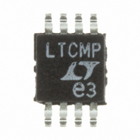
LTC6104CMS8#PBF Linear Technology, LTC6104CMS8#PBF Datasheet

LTC6104CMS8#PBF
Specifications of LTC6104CMS8#PBF
Available stocks
Related parts for LTC6104CMS8#PBF
LTC6104CMS8#PBF Summary of contents
Page 1
... Current Shunt Measurement ■ Battery Monitoring ■ Remote Sensing ■ Power Management , LT, LTC and LTM are registered trademarks of Linear Technology Corporation. All other trademarks are the property of their respective owners. TYPICAL APPLICATION 16-Bit Resolution Bi-Directional Output into LTC1286 ADC I LOAD V SENSE – ...
Page 2
LTC6104 ABSOLUTE MAXIMUM RATINGS (Note 1) Total Supply Voltage (+INB Maximum Applied Output Voltage (OUT) ....................9V Input Current ........................................................±10mA Output Short-Circuit Duration (to V Operating Temperature Range LTC6104C ............................................ –40°C to 85°C LTC6104I ............................................. –40°C to ...
Page 3
ELECTRICAL CHARACTERISTICS temperature range, otherwise specifi cations are ≥ 6V 0.75V for V = 4V, unless otherwise noted. S REF S SYMBOL PARAMETER I Maximum Output Current OUT(MAX) I Current Mirror Gain Error OUT-GAINERR I ...
Page 4
LTC6104 TYPICAL PERFORMANCE CHARACTERISTICS Input V vs Temperature OS 100 TWO REPRESENTATIVE UNITS 100Ω – OUT – 5mV INTERNAL OS –60 AMPLIFIER A V ...
Page 5
TYPICAL PERFORMANCE CHARACTERISTICS Step Response 0mV to 10mV – V SENSE –10mV S 2. 25° 12V 100Ω OUT + SENSE V = ...
Page 6
LTC6104 TYPICAL PERFORMANCE CHARACTERISTICS Step Response Falling Edge – V SENSE – ∆V = 100mV SENSE I = 0µA OUT 6V 5. –100µA OUT T = 25° 12V S = 100Ω ...
Page 7
BLOCK DIAGRAM – OUT THEORY OF OPERATION When V is positive, an internal sense amplifi er loop SENSE forces –INA to have the same potential as +INA. Connect- ing an external resistor series ...
Page 8
LTC6104 APPLICATIONS INFORMATION Selection of External Current Sense Resistor The external sense resistor has a signifi cant effect SENSE on the function of a current sensing system and must be chosen with care. First, the power dissipation in ...
Page 9
APPLICATIONS INFORMATION Selection of External Input Resistor, R The external input resistor controls the trans- IN conductance of the current sense circuit. V SENSE = Since I , transconductance g OUT For example if R ...
Page 10
LTC6104 APPLICATIONS INFORMATION From the Electrical Characteristics of the LTC6104, the output voltage range is 0.3V to 8V. If the circuit that is driven by the output limits the maxi- mum output voltage to ≈5V, to achieve maximum dynamic range, ...
Page 11
APPLICATIONS INFORMATION If the maximum output current, I OUT R equals 3V/1mA = 3k and R = 3k/6 – 0.3Ω (internal OUT IN device resistance) = 499.7Ω. The output error due to DC offset is ±510µV (typ) and the error ...
Page 12
LTC6104 APPLICATIONS INFORMATION the high current path, as this will increase the voltage drop and escalate this error. Output Current Limitations Due to Power Dissipation The LTC6104 can deliver up to ±1mA continuous current to the output pin. This current ...
Page 13
APPLICATIONS INFORMATION Reverse Supply Protection Some applications may be tested with reverse-polarity supplies due to an expectation of this type of fault during operation. The LTC6104 is not protected internally from external reversal of supply polarity. To prevent damage that ...
Page 14
LTC6104 APPLICATIONS INFORMATION decrease the response time, since V Reducing R and increasing R IN OUT effect of increasing the voltage gain of the circuit. Use of Dual Sense Resistors The dual amplifi er topology offers signifi cant advantages for ...
Page 15
... LEAD COPLANARITY (BOTTOM OF LEADS AFTER FORMING) SHALL BE 0.102mm (.004") MAX Information furnished by Linear Technology Corporation is believed to be accurate and reliable. However, no responsibility is assumed for its use. Linear Technology Corporation makes no representa- tion that the interconnection of its circuits as described herein will not infringe on existing patent rights. ...
Page 16
... High Voltage 5V to 100V Operation, SOT23 4V to 60V Operation, Gain Confi gurable with External Resistors ● www.linear.com +INB + V S 6104 TA03 , 55µA Supply Current 0.4V/µs Slew Rate, >1MHz Bandwidth, EE – LT 0107 • PRINTED IN USA © LINEAR TECHNOLOGY CORPORATION 2007 6104f ...


