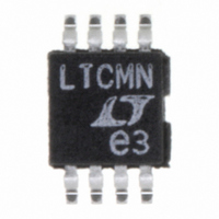
LTC6103IMS8#PBF Linear Technology, LTC6103IMS8#PBF Datasheet

LTC6103IMS8#PBF
Specifications of LTC6103IMS8#PBF
Available stocks
Related parts for LTC6103IMS8#PBF
LTC6103IMS8#PBF Summary of contents
Page 1
... With very low supply current, the LTC6103 is suitable for power sensitive applications. The LTC6103 is available in an 8-lead MSOP package. , LT, LTC and LTM are registered trademarks of Linear Technology Corporation. All other trademarks are the property of their respective owners. 5V 1µF ...
Page 2
LTC6103 ABSOLUTE MAXIMUM RATINGS (Note 1) Total Supply Voltage (+INA/+INB to V Maximum Applied Output Voltage (OUTA/OUTB) ........9V Input Current ........................................................±10mA Output Short-Circuit Duration (to V Operating Temperature Range LTC6103C ............................................ –40°C to 85°C LTC6103I ............................................. –40°C to 85°C LTC6103H ...
Page 3
ELECTRICAL CHARACTERISTICS temperature range, otherwise specifi cations are at T noted. SYMBOL PARAMETER Supply Current per Amplifi er +INA +INB Note 1: Stresses beyond those listed under Absolute Maximum Ratings may cause permanent damage to the device. ...
Page 4
LTC6103 TYPICAL PERFORMANCE CHARACTERISTICS V Maximum vs Temperature OUT 60V 12V –40 – 100 ...
Page 5
TYPICAL PERFORMANCE CHARACTERISTICS Step Response 0mV to 100mV – V SENSE – ∆V =100mV SENSE C = 10pF LOAD 1000pF LOAD T = 25° 12V R = 100Ω OUT ...
Page 6
LTC6103 PIN FUNCTIONS OUTA (Pin 1): Current Output of Amplifi OUTA will source a current that is proportional to the sense voltage of amplifi into an external resistor. OUTB (Pin 2): Current Output of Amplifi er ...
Page 7
THEORY OF OPERATION An internal sense amplifi er loop forces –IN to have the same potential as +IN. Connecting an external resistor between –IN and V forces a potential across R same as the sense voltage across R ...
Page 8
LTC6103 APPLICATIONS INFORMATION Sense Resistor Connection Kelvin connections should be used between the inputs (+IN and –IN) and the sense resistor in all but the lowest power applications. Solder connections and PC board intercon- nections that carry high current can ...
Page 9
APPLICATIONS INFORMATION CMPZ4697 10k M1 Si4465 R SENSE(LO) I LOAD 100mΩ V OUT Figure 3b. The LTC6103 Allows High-Low Current Ranging Care should be taken when designing the printed circuit board layout to minimize input trace resistance (to Pins 5, ...
Page 10
LTC6103 APPLICATIONS INFORMATION Error Sources The current sense system uses an amplifi er and resistors to apply gain and level shift the result. The output is then dependent on the characteristics of the amplifi er, such as bias current and ...
Page 11
APPLICATIONS INFORMATION If the power dissipation of the sense resistor is chosen to be less than 0.5W then: 500 mW ≤ 500 m SENSE 2 I SENSE MAX ( ) • R SENSE(MAX) SENSE(MAX) SENSE ...
Page 12
LTC6103 APPLICATIONS INFORMATION will give a lowpass response. This will reduce unwanted noise from the output, and may also be useful as a charge reservoir to keep the output steady while driving a switch- ing circuit such as a mux ...
Page 13
APPLICATIONS INFORMATION Voltage Translator Each amplifi the LTC6103 can be used as a high volt- age level translator circuit as shown in Figure 7. In this application, the LTC6103 translates a differential voltage signal riding on top of ...
Page 14
LTC6103 TYPICAL APPLICATIONS ±10A Differential Output Bidirectional Current Monitor 10mΩ 200Ω 200Ω BATT 4V < V < 60V BATT +INA –INA –INB + – – – OUTA OUTB V LTC6103 ...
Page 15
... LEAD COPLANARITY (BOTTOM OF LEADS AFTER FORMING) SHALL BE 0.102mm (.004") MAX Information furnished by Linear Technology Corporation is believed to be accurate and reliable. However, no responsibility is assumed for its use. Linear Technology Corporation makes no representa- tion that the interconnection of its circuits as described herein will not infringe on existing patent rights. ...
Page 16
... Operation, Gain Confi gurable with External Resistors ● www.linear.com + DIFFERENTIAL 4.99k OUTPUT + ±2.5V FS (MAY BE LIMITED IF V < 6V) ±10A FS – 4.99k PWM* 6103 TA04 , 55µA Supply Current 0.4V/µs Slew Rate, >1MHz Bandwidth, EE – 6103f LT 0107 • PRINTED IN USA © LINEAR TECHNOLOGY CORPORATION 2007 ...


