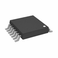
AD8604ARUZ Analog Devices Inc, AD8604ARUZ Datasheet

AD8604ARUZ
Specifications of AD8604ARUZ
Available stocks
Related parts for AD8604ARUZ
AD8604ARUZ Summary of contents
Page 1
FEATURES Low offset voltage: 500 μV maximum Single-supply operation: 2 5.5 V Low supply current: 750 μA/Amplifier Wide bandwidth: 8 MHz Slew rate: 5 V/μs Low distortion No phase reversal Low input currents Unity-gain stable Qualified for automotive ...
Page 2
AD8601/AD8602/AD8604 TABLE OF CONTENTS Features .............................................................................................. 1 Applications....................................................................................... 1 General Description ......................................................................... 1 Pin Configurations ........................................................................... 1 Revision History ............................................................................... 2 Specifications..................................................................................... 3 Electrical Characteristics............................................................. 3 Absolute Maximum Ratings............................................................ 5 Thermal Resistance ...................................................................... 5 ESD Caution.................................................................................. 5 Typical Performance Characteristics ...
Page 3
SPECIFICATIONS ELECTRICAL CHARACTERISTICS / 25°C, unless otherwise noted Table 1. Parameter INPUT CHARACTERISTICS Offset Voltage (AD8601/AD8602) Offset Voltage (AD8604) Input Bias Current Input Offset Current Input Voltage ...
Page 4
AD8601/AD8602/AD8604 25°C, unless otherwise noted Table 2. Parameter INPUT CHARACTERISTICS Offset Voltage (AD8601/AD8602) Offset Voltage (AD8604) Input Bias Current Input Offset Current Input Voltage Range Common-Mode ...
Page 5
ABSOLUTE MAXIMUM RATINGS Table 3. Parameter Supply Voltage Input Voltage Differential Input Voltage Storage Temperature Range Operating Temperature Range Junction Temperature Range Lead Temperature Range (Soldering, 60 sec) ESD Stresses above those listed under Absolute Maximum Ratings may cause permanent ...
Page 6
AD8601/AD8602/AD8604 TYPICAL PERFORMANCE CHARACTERISTICS 3,000 25° 2,500 CM 2,000 1,500 1,000 500 0 –1.0 –0.8 –0.6 –0.4 –0.2 0 0.2 INPUT OFFSET VOLTAGE (mV) Figure 5. Input Offset ...
Page 7
250 200 150 100 50 0 –40 –25 – TEMPERATURE (°C) Figure 11. Input Bias Current vs. Temperature 300 250 200 150 100 50 0 ...
Page 8
AD8601/AD8602/AD8604 10k 25° 100 SOURCE 10 1 0.1 0.001 0.01 0.1 1 LOAD CURRENT (mA) Figure 17. Output Voltage to Supply Rail vs. Load Current 5 5.0 V ...
Page 9
V R 100 PHASE GAIN –20 –40 –60 –80 1k 10k 100k 1M FREQUENCY (Hz) Figure 23. Open-Loop Gain and Phase vs. Frequency A = 100 ...
Page 10
AD8601/AD8602/AD8604 200 25°C 180 A 160 140 120 A = 100 V 100 100 1k 10k 100k FREQUENCY (Hz) Figure 29. Output Impedance vs. Frequency 160 ...
Page 11
1.0 0.8 0.6 0.4 0.2 0 –40 –25 – TEMPERATURE (°C) Figure 35. Supply Current per Amplifier vs. Temperature 1 0.8 0.6 0.4 0.2 0 ...
Page 12
AD8601/AD8602/AD8604 208 25°C A 182 156 130 104 0.5 1.0 1.5 FREQUENCY (kHz) Figure 41. Voltage Noise Density vs. Frequency 25°C A ...
Page 13
10kΩ 200pF 25°C A TIME (400ns/DIV) Figure 47. Large Signal Transient Response 10kΩ 200pF L ...
Page 14
AD8601/AD8602/AD8604 25° 0.1% 0.01% 0 0.1% 0.01% –1 –2 –3 –4 –5 0 200 400 600 SETTLING TIME (ns) Figure 53. Output Swing vs. Settling Time 800 1,000 ...
Page 15
THEORY OF OPERATION The AD8601/AD8602/AD8604 family of amplifiers are rail-to-rail input and output, precision CMOS amplifiers that operate from 2 5 the power supply voltage. These amplifiers use Analog Devices, Inc., DigiTrim® technology to achieve a ...
Page 16
AD8601/AD8602/AD8604 INPUT OVERVOLTAGE PROTECTION As with any semiconductor device condition could exist that could cause the input voltage to exceed the power supply, the device’s input overvoltage characteristic must be considered. Excess input voltage energizes the internal PN ...
Page 17
Voltage drop is created across the 0.1 Ω resistor that is proportional to the load current. This voltage appears at the inverting input of the amplifier due to the feedback correction around the op amp. This creates a current through ...
Page 18
AD8601/AD8602/AD8604 SPICE MODEL The SPICE macro-model for the AD860x amplifier can be down- loaded at www.analog.com. The model accurately simulates a number of both dc and ac parameters, including open-loop gain, bandwidth, phase margin, input voltage range, output voltage swing ...
Page 19
OUTLINE DIMENSIONS 1.70 1.60 1.50 1.30 1.15 0.90 0.15 MAX 0.05 MIN IDENTIFIER 3.00 2.90 2. 3.00 2.80 2. 0.95 BSC 1.90 BSC 0.20 MAX 1.45 MAX 0.08 MIN 0.95 MIN SEATING 0.50 MAX PLANE ...
Page 20
AD8601/AD8602/AD8604 0.25 (0.0098) 0.10 (0.0040) COPLANARITY 4.00 (0.1575) 3.80 (0.1496) 0.25 (0.0098) 0.10 (0.0039) COPLANARITY 0.10 5.00 (0.1968) 4.80 (0.1890 6.20 (0.2441) 4.00 (0.1574) 1 5.80 (0.2284) 3.80 (0.1497) 4 1.27 (0.0500) BSC 1.75 (0.0688) 1.35 (0.0532) 8° ...
Page 21
BSC 4. PIN 1 0.65 BSC 1.05 1.20 1.00 MAX 0.80 0.15 SEATING 0.05 0.30 PLANE COPLANARITY 0.19 0.10 COMPLIANT TO JEDEC STANDARDS MO-153-AB-1 Figure 66. 14-Lead Thin Shrink Small ...
Page 22
... AD8604ARZ-REEL7 −40°C to +125°C AD8604DRZ −40°C to +125°C AD8604DRZ-REEL −40°C to +125°C AD8604ARUZ −40°C to +125°C AD8604ARUZ-REEL −40°C to +125°C AD8604DRU −40°C to +125°C AD8604DRU -REEL −40°C to +125°C AD8604DRUZ −40°C to +125°C AD8604DRUZ-REEL − ...
Page 23
NOTES AD8601/AD8602/AD8604 Rev Page ...
Page 24
AD8601/AD8602/AD8604 NOTES ©20 0–2011 Analog Devices, Inc. All rights reserved. Trademarks and registered trademarks are the property of their respective owners. D01525-0-1/11(G) Rev Page ...


