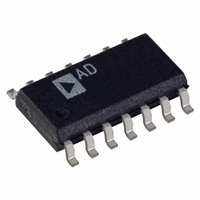
AD8277ARZ Analog Devices Inc, AD8277ARZ Datasheet

AD8277ARZ
Specifications of AD8277ARZ
Available stocks
Related parts for AD8277ARZ
AD8277ARZ Summary of contents
Page 1
FEATURES Wide input range beyond supplies Rugged input overvoltage protection Low supply current: 200 μA maximum per channel Low power dissipation Bandwidth: 550 kHz CMRR minimum kHz ...
Page 2
AD8276/AD8277 TABLE OF CONTENTS Features .............................................................................................. 1 Applications ....................................................................................... 1 General Description ......................................................................... 1 Functional Block Diagram .............................................................. 1 Revision History ............................................................................... 2 Specifications ..................................................................................... 3 Absolute Maximum Ratings ............................................................ 5 Thermal Resistance ...................................................................... 5 Maximum Power Dissipation ..................................................... 5 ...
Page 3
SPECIFICATIONS V = ± ± 25° REF A otherwise noted. Table 2. Parameter Conditions INPUT CHARACTERISTICS 1 System Offset vs. Temperature T = −40°C to +85°C A Average Temperature ...
Page 4
AD8276/AD8277 <± midsupply REF otherwise noted. Table 3. Parameter Conditions INPUT CHARACTERISTICS 1 System Offset vs. Temperature T = −40°C to +85°C A Average Temperature Coefficient T = −40°C to ...
Page 5
ABSOLUTE MAXIMUM RATINGS Table 4. Parameter Supply Voltage Maximum Voltage at Any Input Pin Minimum Voltage at Any Input Pin Storage Temperature Range Specified Temperature Range Package Glass Transition Temperature (T Stresses above those listed under Absolute Maximum Ratings may ...
Page 6
AD8276/AD8277 PIN CONFIGURATIONS AND FUNCTION DESCRIPTIONS REF AD8276 –IN + TOP VIEW +IN OUT 3 6 (Not to Scale) –VS SENSE CONNECT Figure 4. AD8276 8-Lead MSOP Pin Configuration Table ...
Page 7
Table 7. AD8277 Pin Function Descriptions Pin No. Mnemonic Description Connect. 2 −INA Channel A Inverting Input. 3 +INA Channel A Noninverting Input. 4 −VS Negative Supply. 5 +INB Channel B Noninverting Input. 6 −INB Channel B ...
Page 8
AD8276/AD8277 TYPICAL PERFORMANCE CHARACTERISTICS V = ± 25° kΩ connected to ground difference amplifier configuration, unless otherwise noted 2042 MEAN = –2.28 600 SD = 32.7 ...
Page 9
FREQUENCY (Hz) Figure 13. CMRR vs. Frequency 120 100 80 –PSRR 60 +PSRR 100 1k 10k FREQUENCY (Hz) Figure 14. PSRR vs. Frequency ...
Page 10
AD8276/AD8277 +V S –0.2 –0.4 –0.6 –0.8 –1.0 –1.2 +1.2 +1.0 +0.8 +0.6 +0.4 +0.2 – SUPPLY VOLTAGE (±V Figure 19. Output Voltage Swing vs. Supply Voltage Per Channel and Temperature ...
Page 11
I SHORT –5 –10 I SHORT– –15 –20 –50 –30 – TEMPERATURE (°C) Figure 25. Short-Circuit Current Per Channel vs. Temperature 1.4 1.2 –SR 1.0 +SR 0.8 0.6 0.4 ...
Page 12
AD8276/AD8277 ±15V ± 100 1k 10k FREQUENCY (Hz) Figure 31. Maximum Output Voltage vs. Frequency 4.5 4.0 3.5 3.0 2.5 V ...
Page 13
NO LOAD 140 10kΩ LOAD 120 2kΩ LOAD 100 1kΩ LOAD 100 1k FREQUENCY (Hz) Figure 37. Channel Separation 10k 1 00k Rev Page AD8276/AD8277 ...
Page 14
AD8276/AD8277 THEORY OF OPERATION CIRCUIT INFORMATION Each channel of the AD8276/AD8277 consists of a low power, low noise op amp and four laser-trimmed on-chip resistors. These resistors can be externally connected to make a variety of amplifier configurations, including difference, ...
Page 15
POWER SUPPLIES The AD8276/AD8277 operate extremely well over a very wide range of supply voltages. They can operate on a single supply as low and as high under appropriate setup conditions. For best performance, ...
Page 16
AD8276/AD8277 APPLICATIONS INFORMATION CONFIGURATIONS The AD8276/AD8277 can be configured in several ways (see Figure 42 to Figure 46). All of these configurations have excellent gain accuracy and gain drift because they rely on the internal matched resistors. Note that Figure ...
Page 17
The differential output voltage and common-mode voltage of the AD8226 is shown in the following equations − Gain DIFF_OUT +OUT −OUT AD8226 − S− BIAS ...
Page 18
AD8276/AD8277 resistor is determined by the characteristics of the coupler or transformer and desired input voltage ranges to the AD8276. On the voltage monitoring side, potential transformers (PTs) are used to provide coupling and galvanic isolation. The PTs present a ...
Page 19
OUTLINE DIMENSIONS IDENTIFIER 0.25 (0.0098) 0.10 (0.0040) COPLANARITY 3.20 3.00 2.80 5. 3.20 4.90 3.00 4.65 1 2.80 4 PIN 1 0.65 BSC 0.95 15° MAX 0.85 1.10 MAX 0.75 0.15 0.23 6° 0.40 0.05 0.09 0° 0.25 ...
Page 20
... AD8276BRZ-R7 −40°C to +85°C AD8276BRZ-RL −40°C to +85°C AD8277ARZ −40°C to +85°C AD8277ARZ-R7 −40°C to +85°C AD8277ARZ-RL −40°C to +85°C AD8277BRZ −40°C to +85°C AD8277BRZ-R7 −40°C to +85°C AD8277BRZ-RL −40°C to +85° RoHS Compliant Part. © ...


