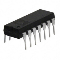
OP470GPZ Analog Devices Inc, OP470GPZ Datasheet - Page 13

OP470GPZ
Manufacturer Part Number
OP470GPZ
Description
IC OPAMP GP 6MHZ QUAD LN 14DIP
Manufacturer
Analog Devices Inc
Specifications of OP470GPZ
Slew Rate
2 V/µs
Amplifier Type
General Purpose
Number Of Circuits
4
Gain Bandwidth Product
6MHz
Current - Input Bias
25nA
Voltage - Input Offset
400µV
Current - Supply
9mA
Voltage - Supply, Single/dual (±)
9 V ~ 36 V, ±4.5 V ~ 18 V
Operating Temperature
-40°C ~ 85°C
Mounting Type
Through Hole
Package / Case
14-DIP (0.300", 7.62mm)
Op Amp Type
General Purpose
No. Of Amplifiers
4
Bandwidth
6MHz
Supply Voltage Range
± 4.5V To ± 18V
Amplifier Case Style
DIP
No. Of Pins
14
Channel Separation
125
Common Mode Rejection Ratio
100
Current, Input Bias
25 nA
Current, Input Offset
12 nA
Current, Supply
9 mA
Impedance, Thermal
33 °C/W
Number Of Amplifiers
Quad
Package Type
PDIP-14
Resistance, Input
0.4 Megohms (Differential), 11 Gigaohms (Common-Mode)
Temperature, Operating, Range
-40 to +85 °C
Voltage, Gain
1700 V/mV
Voltage, Input
±11, ±12 V
Voltage, Noise
3.8 nV/sqrt Hz
Voltage, Offset
0.4 mV
Voltage, Output, High
+13 V
Voltage, Output, Low
-13 V
Voltage, Supply
±15 V
Lead Free Status / RoHS Status
Lead free / RoHS Compliant
Output Type
-
Current - Output / Channel
-
-3db Bandwidth
-
Lead Free Status / Rohs Status
RoHS Compliant part
Electrostatic Device
Available stocks
Company
Part Number
Manufacturer
Quantity
Price
Company:
Part Number:
OP470GPZ
Manufacturer:
AD
Quantity:
1 200
Part Number:
OP470GPZ
Manufacturer:
ADI/亚德诺
Quantity:
20 000
Figure 14. Noise Density of Low Noise Amplifier, G = 1000
DIGITAL PANNING CONTROL
Figure 15 uses a DAC-8408, quad 8-bit DAC to pan a signal
between two channels. The complementary DAC current out-
puts two of the DAC-8408’s four DACs drive current-to-voltage
converters built from a single quad OP470. The amplifiers have
complementary outputs with the amplitudes dependent upon
the digital code applied to the DAC. Figure 16 shows the comple-
mentary outputs for a 1 kHz input signal and digital ramp applied
to the DAC data inputs. Distortion of the digital panning con-
trol is less than 0.01%.
REV. B
100
0%
90
10
SIDE A IN
SIDE B IN
PINS 9 (LSB) – 16 (MSB)
5V
DAC SELECT
DAC DATA BUS
1k
1k
Figure 15. Digital Panning Control Circuit
DAC-8408GP
V
V
A/B
R/W
DS1
DS2
REF
REF
A
C
DGND
DAC A
DAC B
DAC C
DAC D
V
5V
DD
–13–
I
I
OUT2A/2B
OUT2C/2D
I
OUT1A
I
I
I
R
R
R
R
OUT1B
OUT1C
OUT1D
Gain error due to the mismatching between the internal DAC
ladder resistors and the current-to-voltage feedback resistors is
eliminated by using feedback resistors internal to the DAC. Of
the four DACs available in the DAC-8408, only two DACs, A
and C, actually pass a signal. DACs B and D are used to pro-
vide the additional feedback resistors needed in the circuit. If
the VREFB and VREFD inputs remain unconnected, the
current-to-voltage converters using RFBB and RFBD are unaf-
fected by digital data reaching DACs B and D.
FB
FB
FB
FB
A
B
C
D
A OUT
A OUT
Figure 16. Digital Panning Control Output
20pF
20pF
20pF
20pF
100
0%
90
10
1/4
OP470E
1/4
OP470E
1/4
OP470E
1/4
OP470E
5V
+15V
–15V
5V
A OUT
A OUT
B OUT
B OUT
1ms
OP470


