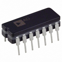
OP470EY Analog Devices Inc, OP470EY Datasheet - Page 11

OP470EY
Manufacturer Part Number
OP470EY
Description
IC OPAMP GP 6MHZ QUAD LN 14CDIP
Manufacturer
Analog Devices Inc
Datasheet
1.OP470GPZ.pdf
(16 pages)
Specifications of OP470EY
Slew Rate
2 V/µs
Rohs Status
RoHS non-compliant
Amplifier Type
General Purpose
Number Of Circuits
4
Gain Bandwidth Product
6MHz
Current - Input Bias
6nA
Voltage - Input Offset
100µV
Current - Supply
9mA
Voltage - Supply, Single/dual (±)
9 V ~ 36 V, ±4.5 V ~ 18 V
Operating Temperature
-25°C ~ 85°C
Mounting Type
Through Hole
Package / Case
14-CDIP (0.300", 7.62mm)
Op Amp Type
General Purpose
No. Of Amplifiers
4
Bandwidth
6MHz
Supply Voltage Range
± 4.5V To ± 18V
Amplifier Case Style
DIP
No. Of Pins
14
Output Type
-
Current - Output / Channel
-
-3db Bandwidth
-
Lead Free Status / RoHS Status
Contains lead / RoHS non-compliant
Available stocks
Company
Part Number
Manufacturer
Quantity
Price
Part Number:
OP470EY
Manufacturer:
PMI
Quantity:
20 000
4. The test time to measure 0.1 Hz to 10 Hz noise should not ex-
5. A noise-voltage-density test is recommended when measuring
6. Power should be supplied to the test circuit by well bypassed
Figure 8. 0.1 Hz to 10 Hz Peak-to-Peak Voltage Noise Test
Circuit Frequency Response
NOISE MEASUREMENT—NOISE VOLTAGE DENSITY
The circuit of Figure 9 shows a quick and reliable method of
measuring the noise voltage density of quad op amps. Each
individual amplifier is series-connected and is in unity-gain, save
the final amplifier which is in a noninverting gain of 101. Since
the ac noise voltages of each amplifier are uncorrelated, they
add in rms fashion to yield:
REV. B
ceed 10 seconds. As shown in the noise-tester frequency-response
curve of Figure 8, the 0.1 Hz corner is defined by only one pole.
The test time of 10 seconds acts as an additional pole to elimi-
nate noise contribution from the frequency band below 0.1 Hz.
noise on a large number of units. A 10 Hz noise voltage-density
measurement will correlate well with a 0.1 Hz to 10 Hz
peak-to-peak noise reading, since both results are determined
by the white noise and the location of the 1/f corner frequency.
low noise supplies, e.g. batteries. These will minimize output
noise introduced via the amplifier supply pins.
100
80
60
40
20
0
0.01
e
OUT
= 101
0.1
Ê
Ë
e
FREQUENCY – Hz
nA
2
1/4
OP470
+ e
1
nB
2
+
e
nC
Figure 9. Noise Voltage Density Test Circuit
2
10
+
1/4
OP470
e
nD
2
ˆ
¯
100
1/4
OP470
–11–
100
The OP470 is a monolithic device with four identical amplifiers.
The noise voltage density of each individual amplifier will match,
giving:
NOISE MEASUREMENT—CURRENT NOISE DENSITY
The test circuit shown in Figure 10 can be used to measure
current noise density. The formula relating the voltage output to
current noise density is:
where:
R1
R1
5
e
V
OUT
S
=
Figure 10. Current Noise Density Test Circuit
(nV Hz) = 101(2e
15V
100k
1/4
OP470
R2
10k
R2
e
OUT
i
G = gain of 10000
R
n
S
=
OP470
DUT
= 100 kW source resistance
TO SPECTRUM ANALYZER
1.24k
=
n
R3
Ê
Á
Ë
)
101
nOUT
200
G
e
R4
OUT
Ê
Ë
ˆ
˜ -
¯
4e
2
n
OP27E
R
2
(
40nV / Hz
S
ˆ
¯
8.06k
= 101 2e
R5
GAIN = 50,000
V
S
=
5V
( )
)
e
SPECTRUM ANALYZER
2
n
n
OP470
OUT TO


