AD524ADZ Analog Devices Inc, AD524ADZ Datasheet - Page 8
AD524ADZ
Manufacturer Part Number
AD524ADZ
Description
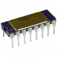
IC AMP INST 1MHZ PREC LN 16CDIP
Manufacturer
Analog Devices Inc
Type
Precisionr
Specifications of AD524ADZ
Amplifier Type
Instrumentation
Number Of Circuits
1
Slew Rate
5 V/µs
Gain Bandwidth Product
1MHz
-3db Bandwidth
1MHz
Current - Input Bias
50nA
Voltage - Input Offset
250µV
Current - Supply
3.5mA
Voltage - Supply, Single/dual (±)
±6 V ~ 18 V
Operating Temperature
-25°C ~ 85°C
Mounting Type
Through Hole
Package / Case
16-CDIP (0.300", 7.62mm)
Bandwidth
25 MHz
Common Mode Rejection Ratio
110
Current, Input Bias
±50 nA
Current, Input Offset
±35 nA
Current, Supply
3.5 mA (Quiescent)
Package Type
SBDIP-16
Power Dissipation
450 mW
Resistance, Input
20 Kilohms
Temperature, Operating, Range
-25 to +85 °C
Voltage, Gain
1-1000 V/V
Voltage, Input
<36 V
Voltage, Input Offset
250 μV
Voltage, Noise
7 nV/sqrt Hz (Input), 90 nV/sqrt Hz (Output)
Voltage, Supply
±15 V
No. Of Amplifiers
5
Input Offset Voltage
250µV
Gain Db Min
1dB
Amplifier Output
Single Ended
Cmrr
110dB
Supply Voltage Range
± 6V To ± 18V
Rohs Compliant
Yes
Lead Free Status / RoHS Status
Lead free / RoHS Compliant
Output Type
-
Current - Output / Channel
-
Lead Free Status / Rohs Status
RoHS Compliant part
Electrostatic Device
Available stocks
Company
Part Number
Manufacturer
Quantity
Price
Company:

Part Number:
AD524ADZ
Manufacturer:
AD
Quantity:
1 000
Company:
Part Number:
AD524ADZ
Manufacturer:
AD
Quantity:
1 000
Part Number:
AD524ADZ
Manufacturer:
ADI/亚德诺
Quantity:
20 000


ABSOLUTE MAXIMUM RATINGS
Table 3.
Parameter
Supply Voltage
Internal Power Dissipation
Input Voltage
Output Short-Circuit Duration
Storage Temperature Range
Operating Temperature Range
Lead Temperature (Soldering, 60 sec)
1
Stresses above those listed under Absolute Maximum Ratings
may cause permanent damage to the device. This is a stress
rating only; functional operation of the device at these or any
other conditions above those indicated in the operational
section of this specification is not implied. Exposure to absolute
maximum rating conditions for extended periods may affect
device reliability.
AD524
OUTPUT
Maximum input voltage specification refers to maximum voltage to which
either input terminal may be raised with or without device power applied.
For example, with ±18 volt supplies maximum, V
voltage maximum, V
+INPUT
RG
–INPUT
(Either Input Simultaneously) |V
(R)
(D, E)
AD524A/AD524B/AD524C
AD524S
NULL
1
OUTPUT
RG
15
16
NULL
1
2
3
2
14
PAD NUMBERS CORRESPOND TO PIN NUMBERS FOR
THE D-16 AND RW-16 16-LEAD CERAMIC PACKAGES.
INPUT
NULL
G = 10
1
4
13
Dimensions shown in inches and (mm)
Contact factory for latest dimensions;
Figure 2. Metallization Photograph
IN
G = 100
5
INPUT
NULL
is ±36 V.
12
G = 1000
11
0.170 (4.33)
IN
| + |V
REFERENCE
S
|
IN
is ±18 V; with zero supply
SENSE
Rating
±18 V
450 mW
<36 V
Indefinite
–65°C to +125°C
–65°C to +150°C
–25°C to +85°C
–55°C to +125°C
+300°C
10
6
9
OUTPUT
8 +V
7 –V
S
S
0.103
(2.61)
Rev. F | Page 8 of 28
ESD CAUTION
NC = NO CONNECT
REFERENCE
INPUT NULL
INPUT NULL
REFERENCE
INPUT NULL
INPUT NULL
OFFSET NULL
OFFSET NULL
– INPUT
+ INPUT
RG
NC
CONNECTION DIAGRAMS
+V
RG
2
–V
+V
+V
INPUT
SOIC (RW-16 and D-16) Packages
INPUT
Figure 4. Leadless Chip Carrier (E)
S
4
5
6
7
8
S
S
2
S
1
2
3
4
5
6
7
8
Figure 3. Ceramic (D) and
3
9
(Not to Scale)
(Not to Scale)
TOP VIEW
AD524
TOP VIEW
10
AD524
4
5
2
7
5
11
1
15
14
19
18
20
12
19
13
16
15
14
13
12
11
10
OUTPUT
OFFSET NULL
OUTPUT
OFFSET NULL
9
–V
RG
OUTPUT NULL
OUTPUT NULL
G = 10
G = 100
G = 1000
SENSE
OUTPUT
–V
18
17
16
15
14
S
S
1
OUTPUT NULL
G = 10
NC
G = 100
G = 1000
SHORT TO
RG
DESIRED
GAIN
2
FOR
SHORT TO
RG
DESIRED
GAIN
2
FOR
Related parts for AD524ADZ
Image
Part Number
Description
Manufacturer
Datasheet
Request
R

Part Number:
Description:
±1.7g Dual-Axis IMEMS Accelerometer Evaluation Board
Manufacturer:
Analog Devices Inc
Datasheet:

Part Number:
Description:
Inertial Sensor Evaluation System
Manufacturer:
Analog Devices Inc
Datasheet:
Part Number:
Description:
Manufacturer:
Analog Devices Inc
Datasheet:
Part Number:
Description:
Manufacturer:
Analog Devices Inc
Datasheet:
Part Number:
Description:
Manufacturer:
Analog Devices Inc
Datasheet:
Part Number:
Description:
Manufacturer:
Analog Devices Inc
Datasheet:
Part Number:
Description:
Manufacturer:
Analog Devices Inc
Datasheet:
Part Number:
Description:
Manufacturer:
Analog Devices Inc
Datasheet:
Part Number:
Description:
Manufacturer:
Analog Devices Inc
Datasheet:
Part Number:
Description:
Manufacturer:
Analog Devices Inc
Datasheet:
Part Number:
Description:
Manufacturer:
Analog Devices Inc
Datasheet:
Part Number:
Description:
Manufacturer:
Analog Devices Inc
Datasheet:
Part Number:
Description:
Manufacturer:
Analog Devices Inc
Datasheet: