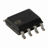
LM833DT STMicroelectronics, LM833DT Datasheet - Page 2

LM833DT
Manufacturer Part Number
LM833DT
Description
IC OP AMP DUAL 8-SOIC
Manufacturer
STMicroelectronics
Datasheet
1.LM833DT.pdf
(12 pages)
Specifications of LM833DT
Amplifier Type
Audio
Number Of Circuits
2
Slew Rate
7 V/µs
Gain Bandwidth Product
15MHz
Current - Input Bias
300nA
Voltage - Input Offset
300µV
Current - Supply
4mA
Voltage - Supply, Single/dual (±)
5 V ~ 30 V, ±2.5 V ~ 15 V
Operating Temperature
-40°C ~ 105°C
Mounting Type
Surface Mount
Package / Case
8-SOIC (3.9mm Width)
Number Of Channels
2
Voltage Gain Db
100 dB
Common Mode Rejection Ratio (min)
80 dB
Input Offset Voltage
5 mV
Operating Supply Voltage
9 V, 12 V, 15 V, 18 V, 24 V, 28 V
Supply Current
8 mA
Maximum Power Dissipation
500 mW
Maximum Operating Temperature
+ 105 C
Mounting Style
SMD/SMT
Maximum Dual Supply Voltage
+/- 15 V
Minimum Operating Temperature
- 40 C
Lead Free Status / RoHS Status
Lead free / RoHS Compliant
Output Type
-
Current - Output / Channel
-
-3db Bandwidth
-
Lead Free Status / Rohs Status
Details
Other names
497-1597-2
Available stocks
Company
Part Number
Manufacturer
Quantity
Price
Company:
Part Number:
LM833DT
Manufacturer:
STMicroelectronics
Quantity:
144 925
Part Number:
LM833DT
Manufacturer:
ST
Quantity:
20 000
Absolute maximum ratings
1
2/12
Absolute maximum ratings
Table 1.
1. Either or both input voltages must not exceed the magnitude of Vcc
2. This input current only exists when the voltage at any of the input leads is driven negative. It is due to the
3. The junction base/substrate of the input PNP transistor polarized in reverse must be protected by a resistor
4. Power dissipation must be considered to ensure maximum junction temperature (Tj) is not exceeded.
5. Human body model: 100 pF discharged through a 1.5 kΩ resistor between two pins of the device, done for
6. Machine model: a 200 pF capacitor is charged to the specified voltage, then discharged directly between
7. Charged device model: all pins plus package are charged together to the specified voltage and then
Table 2.
Symbol
Symbol
collector-base junction of the input PNP transistor becoming forward-biased and thereby acting as input
diode clamp. In addition to this diode action, there is NPN parasitic action on the IC chip. This transistor
action can cause the output voltages of the Op-amps to go to the V
overdrive) for the time during which an input is driven negative.
This is not destructive and normal output is restored for input voltages above -0.3 V.
in series with the inputs to limit the input current to 400 µA max (R = (Vin - 36 V)/400 µA).
all couples of pin combinations with other pins floating.
two pins of the device with no external series resistor (internal resistor < 5 Ω), done for all couples of pin
combinations with other pins floating.
discharged directly to the ground.
T
ESD
V
Ptot
V
T
V
oper
V
I
T
CC
CC
stg
in
id
j
i
Key parameters and their absolute maximum ratings
Operating conditions
Supply voltage
Differential input voltage
Input voltage
Input current
Input current
AMR value
Output short-circuit duration
Junction temperature
Storage temperature
Maximum power dissipation
HBM: human body model
MM: machine model
CDM: charged device model
Supply voltage
Operating free-air temperature range
(1)
(3)
(2)
: V
: V
Parameter
Parameter
in
in
Doc ID 2169 Rev 3
driven positive above
(6)
driven negative
(1)
(5)
(4)
(7)
5 mA in DC or 50 mA in
AC (duty cycle = 10%,
CC
+
or Vcc
voltage level (or to ground for a large
±2.5 to ±15
-65 to +150
±18 or +36
-40 to 105
Infinite
Value
Value
T=1s)
-
+150
.
±30
±15
500
200
0.4
1.5
2
Unit
Unit
mW
mA
°C
kV
kV
°C
°C
V
V
V
V
V
LM833
s


