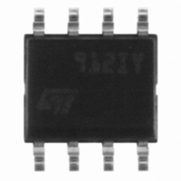
TS912IYDT STMicroelectronics, TS912IYDT Datasheet

TS912IYDT
Specifications of TS912IYDT
Available stocks
Related parts for TS912IYDT
TS912IYDT Summary of contents
Page 1
Features ■ Rail-to-rail input and output voltage ranges ■ Single (or dual) supply operation from 2 ■ Extremely low input bias current typ. ■ Low input offset voltage max. Specified for 600 Ω ...
Page 2
Absolute maximum ratings and operating conditions 1 Absolute maximum ratings and operating conditions Table 1. Absolute maximum ratings Symbol V Supply voltage CC V Differential input voltage id V Input voltage i I Current on inputs in I Current on ...
Page 3
TS912, TS912A, TS912B 2 Schematic diagram Figure 1. Schematic diagram (1/2 TS912 Doc ID 2325 Rev 6 Schematic diagram p 3/20 ...
Page 4
Electrical characteristics 3 Electrical characteristics Table CC+ CC- specified) Symbol Input offset voltage (V TS912 TS912A TS912B V io ≤ T ≤ min amb max TS912 TS912A TS912B ΔV Input offset voltage ...
Page 5
TS912, TS912A, TS912B Table CC+ CC- specified) (continued) Symbol + SR Slew rate ( VCL - SR Slew rate ( VCL φm Phase margin en Equivalent input noise ...
Page 6
Electrical characteristics Table CC+ CC- specified) Symbol Input offset voltage (V TS912 TS912A TS912B V io ≤ T ≤ min amb max TS912 TS912A TS912B ΔV Input offset voltage drift io (1) ...
Page 7
TS912, TS912A, TS912B Table CC+ CC- specified) (continued) Symbol en Equivalent input noise voltage ( Channel separation ( kHz φm Phase margin 1. Maximum values include unavoidable inaccuracies ...
Page 8
Electrical characteristics Table CC+ CC- specified) Symbol Input offset voltage (V TS912 TS912A TS912B V io ≤ T ≤ min amb max TS912 TS912A TS912B ΔV Input offset voltage drift io (1) ...
Page 9
TS912, TS912A, TS912B Table CC+ CC- specified) (continued) Symbol Slew rate + kΩ VCL L Slew rate - ...
Page 10
Electrical characteristics Figure 2. Supply current (each amplifier) vs. supply voltage Figure 4. Low level output voltage vs. low level output current d Figure 6. High level output voltage vs. high level output current d P 10/20 Figure 3. High ...
Page 11
TS912, TS912A, TS912B Figure 8. Gain and phase vs. frequency W Figure 10. Phase margin vs. supply voltage W V Figure 12. Gain bandwidth product vs. supply voltage Figure 9. Figure 11. Gain and phase vs. frequency ...
Page 12
Macromodel Figure 14. Input voltage noise vs. frequency 4 Macromodel 4.1 Important note concerning this macromodel ● All models are a trade-off between accuracy and complexity (i.e. simulation time). ● Macromodels are not a substitute to breadboarding; rather, they confirm ...
Page 13
TS912, TS912A, TS912B 4.2 Macromodel code ** Standard Linear Ics Macromodels, 1993. ** CONNECTIONS : * 1 INVERTING INPUT * 2 NON-INVERTING INPUT * 3 OUTPUT * 4 POSITIVE POWER SUPPLY * 5 NEGATIVE POWER SUPPLY .SUBCKT TS912 1 2 ...
Page 14
Macromodel HSCP 68 25 VSCP1 1E8 DON 69 19 MDTH 400E-12 VON 24 5 2.4419107 HSCN 24 69 VSCN1 1.5E8 VSCTHP 60 61 0.1375 DSCP1 61 63 MDTH 400E-12 VSCP1 ISCP 64 0 1.000000E-8 DSCP2 0 64 ...
Page 15
TS912, TS912A, TS912B 5 Package information In order to meet environmental requirements, ST offers these devices in different grades of ® ECOPACK packages, depending on their level of environmental compliance. ECOPACK specifications, grade definitions and product status are available at: ...
Page 16
Package information 5.1 DIP8 package information Figure 15. DIP8 package mechanical drawing Table 6. DIP8 package mechanical data Ref 16/20 Dimensions Millimeters Min. Typ. Max. 5.33 0.38 ...
Page 17
TS912, TS912A, TS912B 5.2 SO-8 package information Figure 16. SO-8 package mechanical drawing Table 7. SO-8 package mechanical data Ref ccc Dimensions Millimeters Min. Typ. Max. 1.75 ...
Page 18
... Table 8. Order codes Part number TS912IN TS912AIN TS912ID TS912IDT TS912AID TS912AIDT TS912BID TS912BIDT TS912IYD (1) TS912IYDT TS912AIYD (1) TS912AIYDT TS912BIYD (1) TS912BIYDT 1. Qualified and characterized according to AEC Q100 and Q003 or equivalent, advanced screening according to AEC Q001 & Q 002 or equivalent. 18/20 Temperature Package range DIP8 SO-8 -40° ...
Page 19
TS912, TS912A, TS912B 7 Revision history Table 9. Document revision history Date 04-Dec-2001 31-Jul-2005 03-Oct-2005 13-Feb- 2006 16-Oct-2007 01-Feb-2010 Revision 1 First release. PPAP references inserted in the datasheet, see order codes table. 2 ESD protection inserted in AMR table. ...
Page 20
... Information in this document is provided solely in connection with ST products. STMicroelectronics NV and its subsidiaries (“ST”) reserve the right to make changes, corrections, modifications or improvements, to this document, and the products and services described herein at any time, without notice. All ST products are sold pursuant to ST’s terms and conditions of sale. ...


