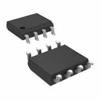
LMV822MX/NOPB National Semiconductor, LMV822MX/NOPB Datasheet - Page 15

LMV822MX/NOPB
Manufacturer Part Number
LMV822MX/NOPB
Description
IC OP AMP R-R LOW VOLT LP 8-SOIC
Manufacturer
National Semiconductor
Datasheet
1.LMV821M5NOPB.pdf
(24 pages)
Specifications of LMV822MX/NOPB
Amplifier Type
General Purpose
Number Of Circuits
2
Output Type
Rail-to-Rail
Slew Rate
2 V/µs
Gain Bandwidth Product
5.6MHz
Current - Input Bias
100nA
Voltage - Input Offset
3500µV
Current - Supply
500µA
Current - Output / Channel
45mA
Voltage - Supply, Single/dual (±)
2.5 V ~ 5.5 V, ±1.25 V ~ 2.75 V
Operating Temperature
-40°C ~ 85°C
Mounting Type
Surface Mount
Package / Case
8-SOIC (3.9mm Width)
Rail/rail I/o Type
Rail to Rail Output
Number Of Elements
2
Unity Gain Bandwidth Product
5.6MHz
Common Mode Rejection Ratio
72dB
Input Offset Voltage
3.5@5VmV
Input Bias Current
100nA
Single Supply Voltage (typ)
2.7/5V
Dual Supply Voltage (typ)
Not RequiredV
Voltage Gain In Db
105dB
Power Supply Rejection Ratio
75dB
Power Supply Requirement
Single
Shut Down Feature
No
Single Supply Voltage (min)
2.5V
Single Supply Voltage (max)
5.5V
Dual Supply Voltage (min)
Not RequiredV
Dual Supply Voltage (max)
Not RequiredV
Operating Temp Range
-40C to 85C
Operating Temperature Classification
Industrial
Mounting
Surface Mount
Pin Count
8
Package Type
SOIC N
Lead Free Status / RoHS Status
Lead free / RoHS Compliant
-3db Bandwidth
-
Lead Free Status / Rohs Status
Compliant
Other names
LMV822MX
LMV822MXTR
LMV822MXTR
Available stocks
Company
Part Number
Manufacturer
Quantity
Price
Company:
Part Number:
LMV822MX/NOPB
Manufacturer:
IXYS
Quantity:
12 456
Part Number:
LMV822MX/NOPB
Manufacturer:
NS/国半
Quantity:
20 000
Application Note
To simplify the design process, certain components are set
equal to each other. Refer to Figure 10 and Figure 11. These
equal component values help to simplify the design equa-
tions as follows:
To illustrate the design process/implementation, a 3 kHz,
Butterworth response, low-pass filter DAAF (Figure 10) is
designed as follows:
1. Choose C
2. Choose R
3. Calculate R
4. Calculate R
Butterworth (Maximally Flat) response is 0.707 (45 degrees
into the s-plane). R
1
4
= R
a
= C
3
and R
for the desired Q. The desired Q for a
3
5
3
= C = 1 nF
= 1 kΩ
calculates as follows:
2
for the desired Fc as follows:
(Continued)
15
Notice that R
The circuit was implemented and its cutoff frequency mea-
sured. The cutoff frequency measured at 2.92 kHz.
The circuit also showed good repeatability. Ten different
LMV822 samples were placed in the circuit. The correspond-
ing change in the cutoff frequency was less than a percent.
TRI-LEVEL VOLTAGE DETECTOR
The tri-level voltage detector of Figure 13 provides a type of
window comparator function. It detects three different input
voltage ranges: Min-range, Mid-range, and Max-range. The
output voltage (V
clamped at GND for the Mid-range. For the Max-range, V
at V
the circuit of Figure 13.
Its operation is as follows: V
the diode bridge to absorb I
tion (V
diode bridge. When this limit is reached, the clamping effect
stops and the op amp responds open loop. The design
equation directly preceding Figure 14, shows how to deter-
mine the clamping range. The equation solves for the input
voltage band on each side GND. The mid-range is twice this
voltage band.
ee
. Figure 14 shows a V
O
= 0V). Eventually, I
3
could also be calculated as 0.707 of R
O
) is at V
IN
IN
O
I
CC
to maintain a clamped condi-
vs. V
deviating from GND, causes
reaches the bias limit of the
for the Min-range. V
I
oscilloscope photo per
10012889
www.national.com
a
or R
O
O
is
is
2.


