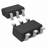
LMH6639MF/NOPB National Semiconductor, LMH6639MF/NOPB Datasheet

LMH6639MF/NOPB
Specifications of LMH6639MF/NOPB
LMH6639MFTR
Available stocks
Related parts for LMH6639MF/NOPB
LMH6639MF/NOPB Summary of contents
Page 1
... The result is a very well behaved frequency response characteristic for any gain setting includ- ing +1, and excellent specifications for driving video cables including harmonic distortion of −60dBc, differential gain of 0.12% and differential phase of 0.045° © 2010 National Semiconductor Corporation LMH6639 Features (V = 5V, Typical values unless specified) S ■ ...
Page 2
... Absolute Maximum Ratings If Military/Aerospace specified devices are required, please contact the National Semiconductor Sales Office/ Distributors for availability and specifications. ESD Tolerance V Differential IN Input Current Supply Voltage (V + – V − ) Voltage at Input/Output pins Storage Temperature Range 3V Electrical Characteristics Unless otherwise specified, all limits guaranteed for at T Boldface limits apply at the temperature extremes ...
Page 3
Symbol Parameter V Output Swing O High Output Swing Low I Output Short Circuit Current SC I Output Current OUT PSRR Power Supply Rejection Ratio I Supply Current (Enabled) S Supply Current (Disabled) TH_SD Threshold Voltage for Shutdown Mode I_SD ...
Page 4
Symbol Parameter TC V Input Offset Average Drift OS I Input Bias Current B I Input Offset Current OS R Common Mode Input IN Resistance C Common Mode Input IN Capacitance CMVR Common-Mode Input Voltage Range CMRR Common Mode Rejection ...
Page 5
Electrical Characteristics Unless otherwise specified, all limits guaranteed for at T Boldface limits apply at the temperature extremes. Symbol Parameter BW −3dB BW BW 0.1dB Gain Flatness 0.1dB FPBW Full Power Bandwidth GBW Gain Bandwidth Product e Input-Referred Voltage ...
Page 6
Symbol Parameter I Output Short Circuit Current SC I Output Current OUT PSRR Power Supply Rejection Ratio I Supply Current (Enabled) S Supply Current (Disabled) TH_SD Threshold Voltage for Shutdown Mode I_SD PIN Shutdown Pin Input Current T On Time ...
Page 7
Ordering Information Package Part Number 6-Pin SOT-23 LMH6639MF LMH6639MFX 8-Pin SOIC LMH6639MA LMH6639MAX Package Marking Transport Media A81A 1k Units Tape and Reel 3k Units Tape and Reel LMH6639MA Rails 2.5k Units Tape and Reel 7 NSC Drawing MF06A M08A ...
Page 8
Typical Performance Characteristics 1kΩ for A = −1. Unless otherwise specified. V Output Sinking Saturation Voltage vs. I for Various Temperature Positive Output Saturation Voltage vs. V for Various Temperature + V from V vs. I OUT www.national.com At T ...
Page 9
I vs. V for Various Temperature vs. V for 3 Representative Units OS S 20030244 V vs. V for 3 Representative Units OS S 20030242 V vs. V for 3 Representative Units OS S 20030232 V vs. ...
Page 10
I vs. V for Various Temperature SUPPLY S Bandwidth for Various V Gain vs. Frequency Normalized www.national.com I vs 20030241 Bandwidth for Various V S 20030206 Gain vs. Frequency Normalized 20030207 10 for Various Temperature S 20030235 S ...
Page 11
Gain Flatness 20030209 Frequency Response vs. Temperature 20030210 Differential Gain/Phase Gain and phase vs. Frequency for Various Temperature Harmonic Distortion On-Off Switching DC Voltage 20030270 11 20030204 20030269 20030211 www.national.com ...
Page 12
On-Off Switching 10MHz Slew Rate (Negative) Power Sweep www.national.com Slew Rate (Positive) 20030212 On-Off Switching of Sinewave 20030213 CMRR vs. Frequency 20030216 12 20030214 20030215 20030218 ...
Page 13
PSRR vs. Frequency 20030217 Voltage Noise 20030219 Off Isolation 20030222 Current Noise Closed Loop Output Resistance vs. Frequency Small Signal Pulse Response (A 13 20030220 20030221 = + 20030250 www.national.com ...
Page 14
Small Signal Pulse Response (A Large Signal Pulse Response www.national.com = −1) Large Signal Pulse Response (R V 20030249 Large Signal Pulse Response 20030227 14 = 2k) L 20030226 20030228 ...
Page 15
Application Notes INPUT AND OUTPUT TOPOLOGY All input / output pins are protected against excessive volt- ages by ESD diodes connected to V+ and V- rails (see 2). These diodes start conducting when the input / output pin voltage approaches ...
Page 16
Note: Pin numbers pertain to SOIC-8 package Multiplexing signals “FREQ 1” and “FREQ 2” exhibit closed loop non-inverting gain of +2 each based upon identical 330Ω resistors in the gain setting positions of IC1 and IC2. The two multiplexing signals ...
Page 17
... Device LMH6639MA LMH6639MF 20030272 These free evaluation boards are shipped when a device sample request is placed with National Semiconductor. For normal operation, tie the SD pin to V 20030273 17 Figure 8 above, Package ...
Page 18
Physical Dimensions www.national.com inches (millimeters) unless otherwise noted 6-Pin SOT23 NS Package Number MF06A 8-Pin SOIC NS Package Number M08A 18 ...
Page 19
Notes 19 www.national.com ...
Page 20
... For more National Semiconductor product information and proven design tools, visit the following Web sites at: www.national.com Products Amplifiers www.national.com/amplifiers Audio www.national.com/audio Clock and Timing www.national.com/timing Data Converters www.national.com/adc Interface www.national.com/interface LVDS www.national.com/lvds Power Management www.national.com/power Switching Regulators www.national.com/switchers LDOs www.national.com/ldo LED Lighting www ...


